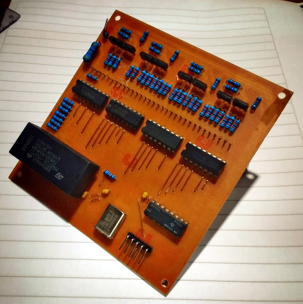
Some time ago, [Bolle] got the idea to redraw the Macintosh SE/30 schematics in Eagle. Progress was initially slow, but over the past month (and with some prodding and assistance from fellow forum frequenter [GeekDot]), he’s taken things a step further by creating a fully functional replacement Macintosh SE/30 logic board PCB.
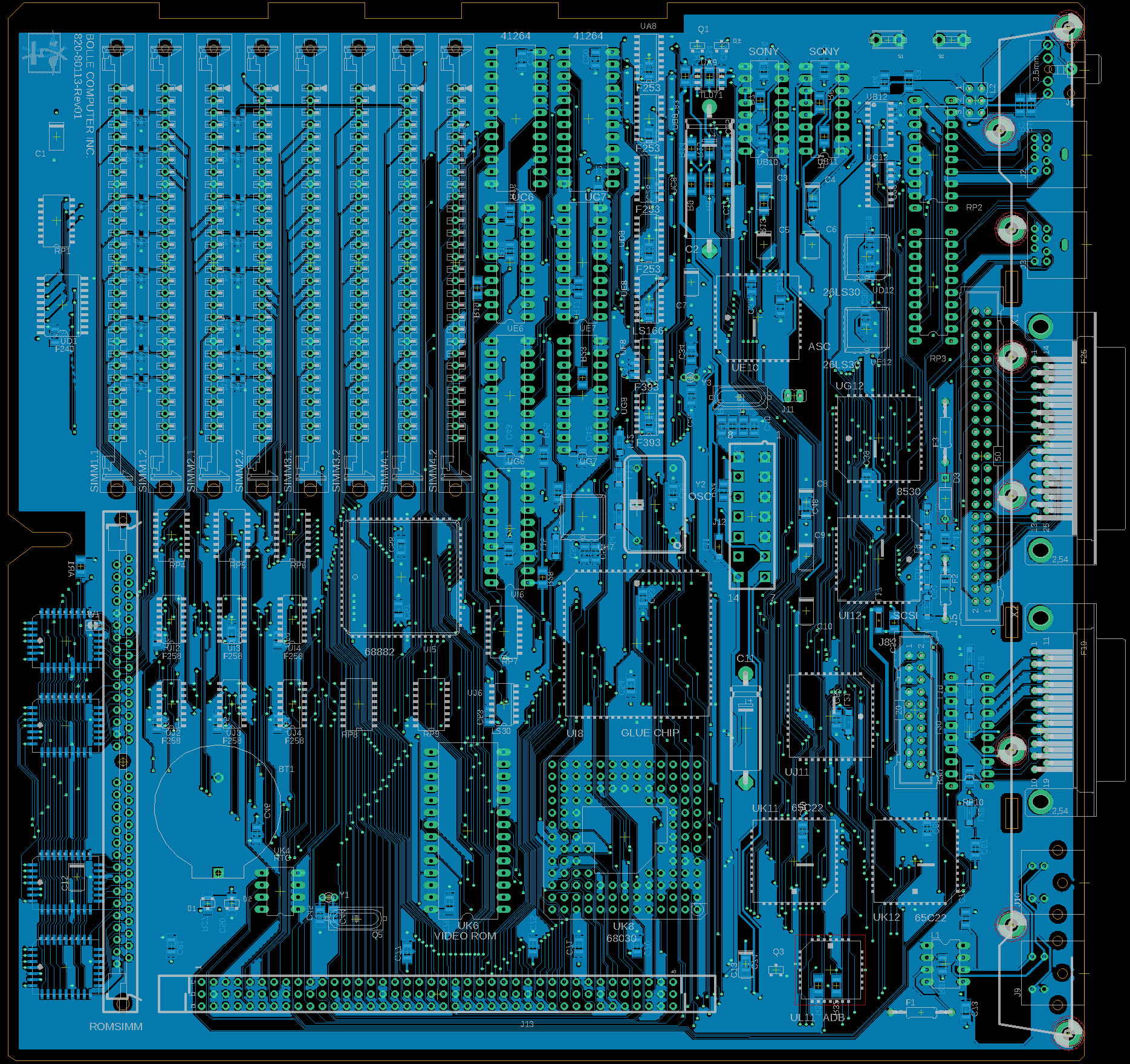
By using the available schematics, the project didn’t even require much reverse engineering. Though he plans for more modernization in later iterations, this design is largely faithful to the original components and layout, ensuring that it is at least basically functional. He did update the real time clock battery to a CR2032 and, as a benefit of redrawing all the traces, he was able to use a 4-layer PCB in place of the costly 6-layer from Apple’s design.
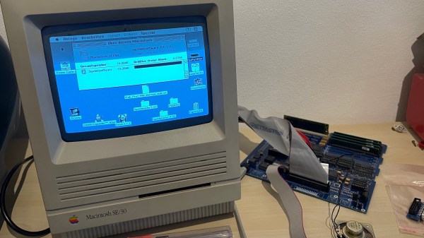
The board came back from fabrication looking beautiful in blue; and, once he had it soldered up and plugged in, the old Mac booted on the very first try! A copy-paste mistake with the SCSI footprints led to some jumper wire bodging in order to get the hard drive working, but that problem has already been fixed in the next revision. And, otherwise, he’s seen no differences from the original after a few hours of runtime.
Recreating old Macintosh logic boards almost seems like its own hobby these days. With the design and fabrication capabilities now accessible to hobbyists, even projects that were once considered professional work are in reach. If you’re interested in making your own PCB designs, there are many resources available to help you get started. Alternatively, we have seen other ways to modernize your classic Macs.
[Thanks to techknight for the tip!]