MeatBagPnP Makes You The Automatic Pick And Place

It’s amazing how hackers are nowadays building increasingly complex hardware with SMD parts as small as grains of sand. Getting multilayer PCB’s and soldering stencils in small quantities for prototyping is easier than ever before. But Pick-and-Place — the process of taking parts and stuffing them on the PCB in preparation for soldering — is elusive, for several reasons. For one, it makes sense only if you plan to do volume production as the cost and time for just setting up the PnP machine for a small run is prohibitive. And a desktop PnP machine isn’t yet as ubiquitous as a 3D printer. Placing parts on the board is one process that still needs to be done manually. Just make sure you don’t sneeze when you’re doing it.

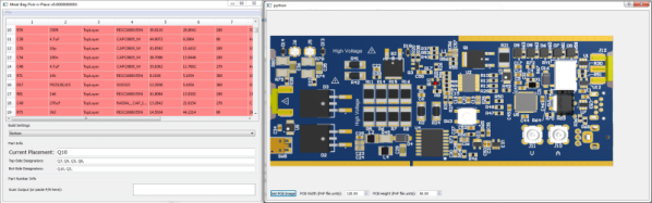
Of course the human is the slow part of this process. [Colin O’Flynn] wrote a python script that he calls MeatBagPnP to ease this bottleneck. It’s designed to look at a row in a parts position file generated from your EDA program and highlight on a render of the board where that part needs to be placed. The human then does what a robotic PnP would have done.

A bar code scanner is not necessary, but using one does make the process a bit quicker. When you scan a code on the part bag, the script highlights the row on the spreadsheet and puts a marker on the first instance of it on the board. After you’ve placed the part, pressing the space bar puts a marker on the next instance of the same value. The script shows it’s done after all parts of the same value are populated and you can then move on to the next part. If you don’t have a bar code scanner handy, you can highlight a row manually and it’ll tell you where to put that part. Check it out in the video below.

Of course, before you use this tool you need some prior preparation. You need a good PNG image of the board (both sides if it is double-sided) scaled so that it is the same dimensions as the target board. The parts position file generated from your EDA tool must use the lower left corner of the board as the origin. You then tell the tool the board dimensions and it scales up everything so that it can put the red markers at the designated XY positions. The script works for single and double-sided boards. For a board with just a few parts, it may not be worth the trouble of doing this, but if you are trying to manually populate a complex board with a lot of parts, using a script like this could make the process a lot less painful.

The project is still fresh and rough around the edges, so if you have comments or feedback to offer, [Colin] is listening.

[Colin]’s name ought to ring a bell — he’s the hacker who built ChipWhisperer which took 2nd Prize at The Hackaday Prize in 2014. The MeatBagPnP project is a result of having worked at building increasingly complex boards manually and trying to make the process easier. In addition to the walk-through of how the script works after the break we’ve embedded his other video from three years back when he was stuffing parts — including BGA’s — the hard way and then reflowing them in a Chinese oven with hacked firmware.

Continue reading “MeatBagPnP Makes You The Automatic Pick And Place”

540 PCBs Make A Giant LED Cube

Just about anyone can make a simple LED cube. But what if you want to make a 1-meter cube using 512 LEDs? [Hari] wanted to do it, so he created two different kinds of LED boards using EasyEDA. There are 270  of each type of board, for a total of 540 (there are only 512 LEDs, so we guess he got some spares due to how the small boards panelized). The goal is to combine these boards to form a cube measuring over three feet on each side.

To simplify wiring, the boards are made to daisy chain like a cordwood module. However, to get things to line up, each column of LED boards have to rotate 90 degrees. You can see several videos about the project below.

Continue reading “540 PCBs Make A Giant LED Cube”

Simulating The Learn-by-Fixing CPU

Last time I looked at a simple 16-bit RISC processor aimed at students. It needed a little help on documentation and had a missing file, but I managed to get it to simulate using a free online tool called EDA Playground. This time, I’ll take you through the code details and how to run the simulation.

You’ll want to refer to the previous post if you didn’t read it already. The diagrams and tables give a high-level overview that will help you understand the files discussed in this post.

If you wanted to actually program this on a real FPGA, you’d have a little work to do. The memory and register initialization is done in a way that works fine for simulation, but wouldn’t work on a real FPGA. Anyway, let’s get started!

Continue reading “Simulating The Learn-by-Fixing CPU”

Learn By Fixing: Another Verilog CPU

Because I often work with students, I’m always on the look-out for a simple CPU, preferably in Verilog, in the Goldilocks zone. That is, not too easy and not too hard. I had high hopes for this 16-bit RISC processor presented by [fpga4student], but without some extra work, it probably isn’t usable for its intended purpose.

The CPU itself is pretty simple and fits on a fairly long web page. However, the details about it are a bit sparse. This isn’t always a bad thing. You can offer students too much help. Then again, you can also offer too little. However, what was worse is one of the modules needed to get it to work was missing! You might argue it was an exercise left to the reader, but it probably should have been pointed out that way.

At first, I was ready to delete the bookmark and move on. Then I decided that the process of fixing this design and doing a little analysis on it might actually be more instructive than just studying a fully working design. So I decided to share my fix with you and look inside the architecture a bit more. On top of that, I’ll show you how to get the thing to run in an online simulator so you can experiment with no software installation. Of course, if you are comfortable with a Verilog toolchain (like the ones from Xilinx or Altera, or even free ones like Icarus or CVer) you should have no problem making that work, either. This time I’ll focus on how the CPU works and next time I’ll show you how to simulate it with some free tools. Continue reading “Learn By Fixing: Another Verilog CPU”

Creating A PCB In Everything: Upverter

For the last five months, I’ve been writing a series of posts describing how to build a PCB in every piece of software out there. Every post in this series takes a reference schematic and board, and recreates all the elements in a completely new PCB tool.

There are three reasons why this sort of review is valuable. First, each post in this series is effectively a review of a particular tool. Already we’ve done Fritzing (thumbs down), KiCad (thumbs up), Eagle (thumbs up), and Protel Autotrax (interesting from a historical perspective). Secondly, each post in this series is a quick getting started guide for each PCB tool. Since the reference schematic and board are sufficiently complex for 90% of common PCB design tasks, each of these posts is a quick how-to guide for a specific tool. Thirdly, this series of posts serves as a basis of comparison between different tools. For example, you can do anything you want in KiCad and most of what you want in Eagle. Fritzing is terrible, and Autotrax is the digital version of the rub-on traces you bought at Radio Shack in 1987.

With that introduction out of the way, let’s get cranking on Upverter.

A little bit about Upverter

Upverter was founded in 2010 as an entirely web-based EDA tool aimed at students, hobbyists, and Open Hardware circuit designers. This was one of the first completely web-based circuit design tools and Upverter’s relative success has been a bellwether for other completely web-based EDA tools such as circuits.io and EasyEDA.

I would like to take a second to mention Upverter is a Y Combinator company (W11), which virtually guarantees this post will make it to the top of Hacker News. Go fight for imaginary Internet points amongst yourselves.

Upverter is a business after all, so how are they making money? Most EDA suites offer a free, limited version for personal, hobbyist, and ‘maker’ projects, and Upverter is no exception. The professional tier offers a few more features including CAM export, 3D preview, an API, simulation (coming soon), BOM management, and unlimited private projects for $125 per seat per month, or $1200 per seat per year.

To give you a basis of comparison for that subscription fee, Eagle CAD’s new license scheme gives you everything – 999 schematic sheets, 16 layers, and unlimited board area – for $65 per month, or $500 per year. Altium’s CircuitStudio comes in at $1000 for a one-year license. There are more expensive EDA suites such as Altium Designer and OrCAD, but you have to call a sales guy just to get a price.

Upverter is positioning itself as a professional tool at a professional price. There are better tools out there, of course, but there are thousands of businesses out there designing products with tools that cost $500 to $1000 per seat per year. In any event, this is all academic; the Hackaday crowd gravitates towards the free end of the market, whether that means beer or speech.

A big draw for Upverter is their Parts Concierge service. You’ll never have to create a part from scratch again, so the sales copy says. Apparently, Upverter is using a combination of very slick scripts to pull part layouts off a datasheet and human intervention / sanity check to create these parts. Does it work? We’re going to find out in the review below.

Continue reading “Creating A PCB In Everything: Upverter”

Friday Hack Chat: KiCad EDA Suite With Wayne Stambaugh

KiCad is the premiere open source electronics design automation suite. It’s used by professionals and amateurs alike to design circuits and layout out printed circuit boards. In recent years we’ve seen some incredible features added to KiCad like an improved 3D viewer and push-and-shove routing. This Friday at 10 am PST, join in a Hack Chat with KiCad lead developer [Wayne Stambaugh] to talk about recent improvements and what the team has planned for KiCad in the future.

[Wayne] has been an electronics engineer for over 30 years with a wide range of experience in analog and digital hardware design and embedded and application software design. He started hacking on KiCad ten years ago when the project was first opened to public development and a little over two years ago became the project leader. This is an excellent opportunity to learn how the development team works, what their current goals are, and to talk all things KiCad.

Don’t miss this Hack Chat! Here’s a handy web tool to help convert Jan. 20 at 10:00 am PST to your local time.

Wait, There’s Tindie Too!

Also on Friday, taking place just an hour before the KiCad chat, is a Tindie Hack Chat. All are welcome as the 9:00 am PST discussion gets under way. Discussion will focus on all aspects of selling unique hardware on Tindie.

Here’s How to Take Part:

join-project-team-message-buttons
Buttons to join the project and enter Hack Chat

Hack Chat are live community events that take place in the Hackaday.io Hack Chat group messaging. Visit that page (make sure you are logged in) and look for the “Join this Project Button” in the upper right. Once you are part of the project, that button will change to “Team Messaging” which takes you to the Hack Chat.

You don’t have to wait for Friday, join Hack Chat whenever you like and see what the community is currently talking about.

 Join Us Next Week Too for CircuitPython

Block out your calendar for noon PST on Friday the 27th for next week’s Hack Chat. Joining us are Adafruit’s Ladyada, Tony DiCola, and Scott Shawcoft. They’ll be leading a discussion about CircuitPython Beta, Adafruits new extension to MicroPython that adds SAMD21 support and other enhancements.

Friday Hack Chat: Eagle PCB Design With Matt Berggren

Eagle is a household name for all Hackaday regulars. Here’s your chance to learn about upcoming features, get your ‘how do I do this in Eagle?’ questions answered, and get your wishlist items heard. Join us on Friday at 12:00 PST for a live Hack Chat about the Eagle PCB Design software.

Hosting this week’s discussion is [Matt Berggren], also known on Hackaday.io as technolomaniac. Matt is the Director of Autodesk Circuits and with Autodesk’s acquisition of Eagle last summer, the popular schematic design and PCB layout software falls under his purview. He has an extensive background in designing printed circuit boards — if you can do it in EDA software he knows how — this is an excellent opportunity to get answered the questions that have been stumping you.

Don’t miss this Hack Chat! Here’s a handy web tool to help convert 1/13/17 at 12:00 PST to your local time.

Here’s How to Take Part:

join-project-team-message-buttons
Buttons to join the Hacker Channel and enter Hack Chat

Hack Chat are live community events that take place in the Hackaday.io Hacker Channel. Visit that page (make sure you are logged in) and look for the “Join this Project Button” in the upper right. Once you are part of the Hacker Channel, that button will change to “Team Messaging” which takes you to the Hack Chat.

You don’t have to wait for Friday, join Hack Chat whenever you like and see what the community is currently talking about.

Join Us Next Week Too for KiCad!

Are you more of a KiCad person than an Eagle person? You should still drop by this week to see if Matt changes your mind. But block out your calendar next week when [Wayne Stambaugh], one of the lead developers of KiCad will join us for a Hack Chat on Friday, 1/20/17.