As part of writing tech stories such as those we feature here at Hackaday, there is a huge amount of research to be done. We trawl through pages and pages of obscure blogs, videos, and data sheets. Sometimes we turn up resources interesting enough that we file them away, convinced that they contain the nucleus of another story at some point in the future.
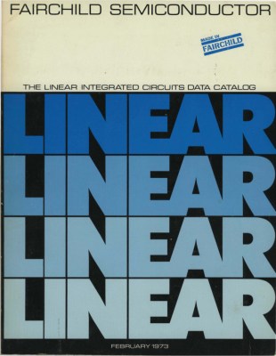 Today’s topic of entertainment is just such a resource, courtesy of the Internet Archive. It’s not a video as we’d often provide you in a Retrotechtacular piece, instead it’s the February 1973 edition of the Fairchild Semiconductor Linear Integrated Circuits Catalog. Books like this one that could be had from company sales representatives were highly prized in the days before universal Internet access to data sheets, and the ink-on-paper datasheets within it provide a fascinating snapshot of the integrated electronics industry as it was 45 years ago.
The first obvious difference between then and now is one of scale, this is a single volume containing Fairchild’s entire range. At 548 pages it wouldn’t have been a slim volume by any means, but given that Fairchild were at the time one of the big players in the field it is unimaginable that the entire range of a 2018 equivalent manufacturer could be contained in the same way. Given that the integrated circuit was at the time an invention barely 15 years old, we are looking at an industry still in relative infancy.
The catalog has a series of sections with familiar headings: Operational amplifiers, comparators, voltage regulators, computer/interface, consumer, and transistor/diode arrays with analog switches. Any modern catalog will have similar headings, and there are even a few devices you will find have survived the decades. The μA741 op-amp (page 64) from its original manufacturer has not yet become a commodity product here, and it sits alongside familiar devices such as the μA7800 series (page 201) or μA723 (page 194) regulators.
Continue reading “Retrotechtacular: AM Radios, Core Memory, And Color TV, What Was Hot In Chips In ’73” →