EcoEDA Integrates Your Junk Bin Into Your Designs

If you’re like us, there’s a creeping feeling that comes over you when you’re placing an order for parts for your latest project: Don’t I already have most of this stuff? With the well-stocked junk bins most of us sport and the stacks of defunct electronics that are almost always within arm’s length, chances are pretty good you do. And yet, we always seem to just click the button and place a new order anyway; it’s just easier.

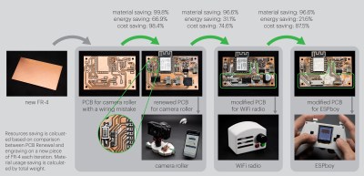
But what if mining the treasure in your junk bin was easier? If you knew right at design time that you had something in your stash you could slot into your build, that would be something, right? That’s the idea behind ecoEDA, a Python-based KiCAD plugin by [Jasmine Lu], [Beza Desta], and [Joyce Passananti]. The tool integrates right into the schematic editor of KiCAD and makes suggestions for substitutions as you work. The substitutions are based on a custom library of components you have on hand, either from salvaged gear or from previous projects. The plug-in can make pin-for-pin substitutions, suggest replacements with similar specs but different pinouts, or even build up the equivalent of an integrated circuit from available discrete components. The video below gives an overview of the tool and how it integrates into the design workflow; there’s also a paper (PDF) with much more detail.

This seems like an absolutely fantastic idea. Granted, developing the library of parts inside all the stuff in a typical junk bin is likely the biggest barrier to entry for something like this, and may be too daunting for some of us. But there’s gold in all that junk, both literally and figuratively, and putting it to use instead of dumping it in a landfill just makes good financial and environmental sense. We’re already awash in e-waste, and anything we can do to make that even just a little bit better is probably worth a little extra effort. Continue reading “EcoEDA Integrates Your Junk Bin Into Your Designs”

Designing A PCB GPS Antenna From Scratch

These days, when it comes to GPS devices the antenna is typically part of the package. But what better opportunity for [Pepijn] to learn how to make a GPS antenna from scratch for a badge add-on?

A patch antenna is an antenna of a flat design, which [Pepijn] was going to put directly on a PCB. However, there was added complexity due to GPS being a circularly polarized signal, and that meant doing some research.

Sadly, nowhere did [Pepijn] encounter a straightforward reference design or examples, but in the end success came from going with a truncated corner patch antenna design and using simulation software to figure out exactly what dimensions were needed. (The openEMS free simulation software didn’t bring success, but the non-free Sonnet with a trial license did the trick.) The resulting PCB may not look particularly complex, but every detail matters in such designs.

KiCad handled the PCB CAD design but the prototype came from cutting the PCB on a CNC machine instead of having it fabricated and shipped; a much cheaper and faster option for those with access to the right tools. A bit more testing had the prototype looking good, but the real proof came when it successfully received GPS signals and spewed valid NMEA messages. The design files are on GitHub but as [Pepijn] says, the project was about the journey more than anything else.

Chip Shortage Engineering: Misusing DIP Packages

After years of seeing people showing off and trading their badge Simple Add-Ons (SAOs) at Supercon, this year I finally decided to make one myself. Now for a first attempt, it would have been enough to come up with some cool PCB art and stick a few LEDs on it. But naturally I started with a concept that was far more ambitious than necessary, and before long, had convinced myself that the only way to do the thing justice was to have an onboard microcontroller.

My first thought was to go with the venerable ATtiny85, and since I already had a considerable stock of the classic eight-pin DIP MCUs on hand, that’s what I started prototyping with. After I had something working on the breadboard, the plan was to switch over to the SOIC-8 version of the chip which would be far more appropriate for something as small as an SAO.

Unfortunately, that’s where things got tricky. I quickly found that none of the major players actually had the SMD version of the chip in stock. Both DigiKey and Mouser said they didn’t expect to get more in until early 2024, and while Arrow briefly showed around 3,000 on hand, they were all gone by the time I checked back. But that was only half the problem — even if they had them, $1.50 a piece seems a hell of a lot of money for an 8-bit MCU with 8K of flash in 2023.

The whole thing was made all the more frustrating by the pile of DIP8 ATtiny85s sitting on the bench, mocking me. Under normal circumstances, using them in an SAO wouldn’t really be a problem, but eight hand-soldered leads popping through the front artwork would screw up the look I had in mind.

While brooding over the situation my eyes happened to fall on one of the chips I had been fiddling with, it’s legs badly bent from repeated trips through the programmer. Suddenly it occurred to me that maybe there was a way to use the parts I already had…

Continue reading “Chip Shortage Engineering: Misusing DIP Packages”

Thin Keyboard Fits In Steam Deck Case

Although some of the first Android-powered smartphones had them and Blackberries were famous for them, physical keyboards on portable electronics like that quickly became a thing of the past. Presumably the cost to manufacture is too high and the margins too low regardless of consumer demand. Whatever the reason, if you want a small keyboard for your portable devices you’ll likely need to make one yourself like [Kārlis] did for the Steam Deck.

Unlike a more familiar mechanical keyboard build which prioritizes the feel and sound of the keyboard experience, this one sacrifices nearly every other design consideration in order to be thin enough to fit in the Steam Deck case. The PCB is designed to be flexible using copper tape cut to size with a vinyl cutter with all the traces running to a Raspberry Pi Pico which hosts the firmware and plugs into the Steam Deck’s USB port. The files for the PCB are available in KiCad and can be exported as SVG files for cutting.

In the end, [Kārlis] has a functioning keyboard that’s even a little more robust than was initially expected and which does fit alongside the Deck in its case. On the other hand, [Kārlis] describes the typing experience as “awful” due to its extreme thinness, but either way we applaud the amount of effort that went in to building a keyboard with this form factor. The Steam Deck itself is a platform which lends itself to all kinds of modifications as well, from the control sticks to the operating systems, and Valve will even show you how.

Hackaday Prize 2023: Jumperless, The Jumperless Jumperboard

Jumperless is a jumperless breadboard with multicolored LED visualization of signals in real-time. Sounds like magic? This beautifully executed entry to the 2023 Hackaday Prize by [Kevin Santo Cappuccio] uses a boatload of CH446Q analog switch ICs to perform the interconnect between the Raspberry Pi Pico header and the jumper board (or breadboard if you prefer.)

This will add some significant resistance, but for low currents and digital logic levels, this should not be a major concern. Additionally, there are two DAC channels and four ADC channels to help break out of the digital world, which could make for some very interesting non-trivial applications.

The visualization of the Pico header signals is solved neatly with a tiny wishbone-shaped PCB that is reverse-mounted to the back of the main board to illuminate upwards. The masking of the labels is done by using copper to mask off the individual signals and solder mask to draw in the legends. This PCB-level hacking is simply wonderful to see. The PCBs are designed with KiCAD, the design files for which you can find here. It appears however that [Kevin] needed to have the spring clips for the jumper board custom-made, so you’d need to contact them if you needed to get some for a build.

On the software side of things, [Kevin] currently recommends using Wokwi, to run the Arduino stack applications and to perform the signal routing to the virtual jumper board. You can follow how it works internally here. A Python-based bridge application runs on the host computer, which takes care of programming the interconnects as they are constructed, which looking at the demo in the embedded video, appears to ‘just work.’

One word of caution though — the bridge app uses Python requests and Beautiful Soup to scrape the Wowki project page, which could potentially make it vulnerable to getting out-of-sync with updates, so hopefully [Kevin] will keep track of this and keep them in sync.

Need some breadboarding tips? We got you covered. Talking of bread, here’s an 8-bit TTL breadboard-based CPU in a breadbin.

Continue reading “Hackaday Prize 2023: Jumperless, The Jumperless Jumperboard”

Where Did Your PCB Go Wrong? KiRI Knows

When working on a PCB design in KiCad, it’s helpful that the files are all text and can easily be checked into Git or other source control. However, stepping back through the revisions to determine where precisely a trace got routed wrong can be tricky. [Leandro] started with a simple script that exported the KiCad project to an image for inspection — over time it grew into a full-blown visual diff tool named KiCad Revision Inspector (KiRI).

The primary mechanism exports the revisions of a KiCad 5, 6, or 7 project to SVG, which can then be compared via a handy onion skin view. As this is a tool written for those using KiCad, shortcuts are a huge part of the experience. A command line interface generates artifacts to view the diff in any web browser. As these outputs have the KiRI tooling baked in, it is relatively easy to archive the output as a build artifact and allow easy access to review design changes.

For the long-time reader, you might remember back in 2018 talked about another diffing tool called plotgitsch (which this KiRI uses for KiCad 5 projects). KiCad has grown significantly in the last five years. It might be time to update our tips to utilize Git better for your PCB designs.

Continue reading “Where Did Your PCB Go Wrong? KiRI Knows”

Hackaday Prize 2023: Circuit Scout Lends A Hand (Or Two) For Troubleshooting

Troubleshooting a circuit is easy, right? All you need is a couple of hands to hold the probes, another hand to twiddle the knobs, a pair of eyes to look at the schematic, another pair to look at the circuit board, and, for fancy work, X-ray vision to see through the board so you know what pads to probe. It’s child’s play!

In the real world, most of us don’t have all the extra parts needed to do the job right, which is where something like CircuitScout would come in mighty handy. [Fangzheng Liu] and [Thomas Juldo]’s design is a little like a small pick-and-place machine, except that instead of placing components, the dual gantries place probes on whatever test points you need to look at. The stepper-controlled gantries move independently over a fixture to hold the PCB in a known position so that the servo-controlled Z-axes can drive the probes down to the right place on the board.

As cool as the hardware is, the real treat is the software. A web-based GUI parses the PCB’s KiCAD files, allowing you to pick a test point on the schematic and have the machine move a probe to the right spot on the board. The video below shows CircuitScout moving probes from a Saleae logic analyzer around, which lets you both control the test setup and see the results without ever looking away from the screen.

CircuitScout seems like a brilliant idea that has a lot of potential both for ad hoc troubleshooting and for more formal production testing. It’s just exactly what we’re looking for in an entry for the Gearing Up round of the 2023 Hackaday Prize.

Continue reading “Hackaday Prize 2023: Circuit Scout Lends A Hand (Or Two) For Troubleshooting”