NES Zapper Becomes Telephone

Although there was a time in the 80s (and early 90s for fans of the SuperScope) where light guns were immensely popular, with games like DuckHunt cultural touchstones, their time in the video game world has largely come to an end. We might occasionally pick up a Zapper for the NES and play this classic out of nostalgia, but plenty of people are looking for other things that these unique video game controllers can do instead. [Nick] has turned one of his old NES peripherals into a wireless phone.

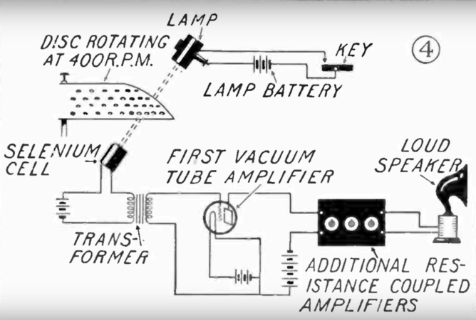
The way the original Zapper worked was by looking for a certain pattern of pixels that displayed for a fraction of a second whenever the trigger was pulled. Bypassing the anti-cheat mechanism that looks only for qualities of light coming from CRT screens of the day effectively turns the light gun into an analog light sensor which is used for receiving the audio from the phone’s base station via a laser. Of course there were no microphones present within the original hardware so one is added, wiring its output to another laser that communicates to the base station. With the light gun pointed directly at this base station, audio is communicated back and forth by varying the strengths of these small lasers and listening to them on the other end with photodiodes.

[Nick] does point out that this isn’t a great phone, largely because it needs to be pointed exactly at the right spot to work at all, although we do agree that it’s an interesting project that demonstrates what the original hardware could do with a few of its limitations removed. There are a few other ways of bringing these devices into the modern world, with one of our favorites being this laser pointer with additional hardware from a Wiimote that could also function as a mouse.

Continue reading “NES Zapper Becomes Telephone”

Shine On You Crazy Diamond Quantum Magnetic Sensor

We’re probably all familiar with the Hall Effect, at least to the extent that it can be used to make solid-state sensors for magnetic fields. It’s a cool bit of applied physics, but there are other ways to sense magnetic fields, including leveraging the weird world of quantum physics with this diamond, laser, and microwave open-source sensor.

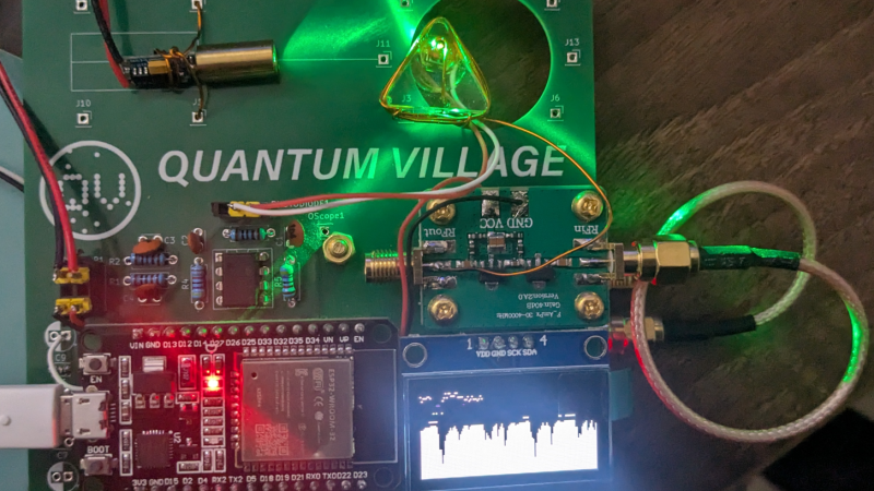
Having never heard of quantum sensors before, we took the plunge and read up on the topic using some of the material provided by [Mark C] and his colleagues at Quantum Village. The gist of it seems to be that certain lab-grown diamonds can be manufactured with impurities such as nitrogen, which disrupt the normally very orderly lattice of carbon atoms and create a “nitrogen vacancy,” small pockets within the diamond with extra electrons. Shining a green laser on N-V diamonds can stimulate those electrons to jump up to higher energy states, releasing red light when they return to the ground state. Turning this into a sensor involves sweeping the N-V diamond with microwave energy in the presence of a magnetic field, which modifies which spin states of the electrons and hence how much red light is emitted.

Building a practical version of this quantum sensor isn’t as difficult as it sounds. The trickiest part seems to be building the diamond assembly, which has the N-V diamond — about the size of a grain of sand and actually not that expensive — potted in clear epoxy along with a loop of copper wire for the microwave antenna, a photodiode, and a small fleck of red filter material. The electronics primarily consist of an ADF4531 phase-locked loop RF signal generator and a 40-dB RF amplifier to generate the microwave signals, a green laser diode module, and an ESP32 dev board.

All the design files and firmware have been open-sourced, and everything about the build seems quite approachable. The write-up emphasizes Quantum Village’s desire to make this quantum technology’s “Apple II moment,” which we heartily endorse. We’ve seen N-V sensors detailed before, but this project might make it easier to play with quantum physics at home.

Laser Harp Sets The Tone

In many ways, living here in the future is quite exiting. We have access to the world’s information instantaneously and can get plenty of exciting tools and hardware delivered to our homes in ways that people in the past with only a Sears catalog could only dream of. Lasers are of course among the exciting hardware available, which can be purchased with extremely high power levels. Provided the proper safety precautions are taken, that can lead to some interesting builds like this laser harp which uses a 3W laser for its strings.

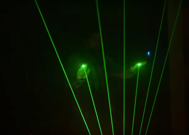
[Cybercraftics]’ musical instrument is using a single laser to generate seven harp strings, using a fast stepper motor to rotate a mirror to precise locations, generating the effect via persistence of vision. Although he originally planned to use one Arduino for this project, the precise timing needed to keep the strings in the right place was getting corrupted by adding MIDI and the other musical parts to the project, so he split those out to a second Arduino.

Although his first prototype worked, he did have to experiment with the sensors used to detect his hand position on the instrument quite a bit before getting good results. This is where the higher power laser came into play, as the lower-powered ones weren’t quite bright enough. He also uses a pair of white gloves which help illuminate a blocked laser. With most of the issues ironed out, [Cybercraftics] notes that there’s room for improvement but still has a working instrument that seems like a blast to play. If you’re still stuck in the past without easy access to lasers, though, it’s worth noting that there are plenty of other ways to build futuristic instruments as well.

Continue reading “Laser Harp Sets The Tone”

DIY laser microphone on cutting mat

Spy Tech: Build Your Own Laser Eavesdropper

Laser microphones have been around since the Cold War. Back in those days, they were a favorite tool of the KGB – allowing spies to listen in on what was being said in a room from a safe distance. This project by [SomethingAbtScience] resurrects that concept with a DIY build that any hacker worth their soldering iron can whip up on a modest budget. And let’s face it, few things are cooler than turning a distant window into a microphone.

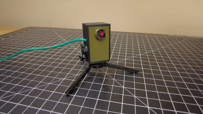
At its core this hack shines a laser on a window, detects the reflected light, and picks up subtle vibrations caused by conversations inside the room. [SomethingAbtScience] uses an ordinary red laser (visible, because YouTube rules) and repurposes an amplifier circuit ripped from an old mic, swapping the capsule for a photodiode. The build is elegant in its simplicity, but what really makes it shine is the attention to detail: adding a polarizing filter to cut ambient noise and 3D printing a stabilized sensor mount. The output is still a bit noisy, but with some fine tuning – and perhaps a second sensor for differential analysis – there’s potential for crystal-clear audio reconstruction. Just don’t expect it to pass MI6 quality control.

While you probably won’t be spying on diplomats anytime soon, this project is a fascinating glimpse into a bygone era of physical surveillance. It’s also a reminder of how much can be accomplished with a laser pointer, some ingenuity, and the curiosity to see how far a signal can travel.

Continue reading “Spy Tech: Build Your Own Laser Eavesdropper”

Got Junk? Then Build This Scrappy TEA Laser

A piece of glass, some bits of tinfoil, a sheet of plastic, a couple of razor blades, and a few assorted bits and bobs are all it takes to build this TEA nitrogen laser. Oh, and a 5,000-volt flyback supply with enough amperage to stop your heart. You’ll need that too.

Seriously, if you choose to follow [MultiverseCurator] ‘s example and build this laser, you’ll want to take the proper precautions. A transversely excited atmospheric laser is simple in concept, but there are plenty of ways for them to go wrong. Unlike the gas lasers used in laser cutters, there’s no enclosed resonator cavity or mirrors. Rather, the excitation takes place across a narrow gap between two electrodes, using atmospheric nitrogen as the lasing medium. This results in hard UV emissions, which means you can’t see them with the naked eye. Add to that the spark gap creating extremely loud discharges as the laser operates, and hazards abound. Proceed with caution.

Construction starts with a flat glass plate and a pair of large capacitors made from aluminum foil plates separated by a plastic dielectric. The razor blades are connected across the capacitors, separated by a narrow gap, with an inductor made from magnet wire in parallel. A spark gap made from nuts and bolts goes in series, and the whole assembly gets connected to a high-voltage power supply — [Multiverse] used a ZVS driver and a CRT flyback transformer with an eight-megohm resistor in series. The video below has all the build details.

It’ll take a little fiddling to get it lasing, and you’ll need something phosphorescent to see the UV light — a scrap of copy paper should do. But the results are pretty amazing for something made from scrap. If you want to take the design to the next level, you’ll want to check out [Les Wright]’s TEA laser build.

Continue reading “Got Junk? Then Build This Scrappy TEA Laser”

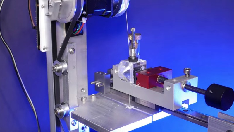
Pulsed Deposition Points A Different Path To DIY Semiconductors

While not impossible, replicating the machines and processes of a modern semiconductor fab is a pretty steep climb for the home gamer. Sure, we’ve seen it done, but nanoscale photolithography is a demanding process that discourages the DIYer at every turn. So if you want to make semiconductors at home, it might be best to change the rules a little and give something like this pulsed laser deposition prototyping apparatus a try.

Rather than building up a semiconductor by depositing layers of material onto a silicon substrate and selectively etching features into them with photolithography, [Sebastián Elgueta]’s chips will be made by adding materials in their final shape, with no etching required. The heart of the process is a multi-material pulsed laser deposition chamber, which uses an Nd:YAG laser to ablate one of six materials held on a rotating turret, creating a plasma that can be deposited onto a silicon substrate. Layers can either be a single material or, with the turret rapidly switched between different targets, a mix of multiple materials. The chamber is also equipped with valves for admitting different gases, such as oxygen when insulating layers of metal oxides need to be deposited. To create features, a pattern etched into a continuous web of aluminum foil by a second laser is used as a mask. When a new mask is needed, a fresh area of the foil is rolled into position over the substrate; this keeps the patterns in perfect alignment.

We’ve noticed regular updates on this project, so it’s under active development. [Sebastián]’s most recent improvements to the setup have involved adding electronics inside the chamber, including a resistive heater to warm the substrate before deposition and a quartz crystal microbalance to measure the amount of material being deposited. We’re eager to see what else he comes up with, especially when those first chips roll off the line. Until then, we’ll just have to look back at some of [Sam Zeloof]’s DIY semiconductors.

Growing A Gallium-Arsenide Laser Directly On Silicon

As great as silicon is for semiconductor applications, it has one weakness in that using it for lasers isn’t very practical. Never say never though, as it turns out that you can now grow lasers directly on the silicon material. The most optimal material for solid-state lasers in photonics is gallium-arsenide (GaAs), but due to the misalignment of the crystal lattice between the compound (group III-V) semiconductor and silicon (IV) generally separate dies would be produced and (very carefully) aligned or grafted onto the silicon die.

Naturally, it’s far easier and cheaper if a GaAs laser can be grown directly on the silicon die, which is what researchers from IMEC now have done (preprint). Using standard processes and materials, GaAs lasers were grown on industry-standard 300 mm silicon wafers. The trick was to accept the lattice mismatch and instead focus on confining the resulting flaws through a layer of silicon dioxide on top of the wafer. In this layer trenches are created (see top image), which means that when the GaAs is deposited it only contacts the Si inside these grooves, thus limiting the effect of the mismatch and confining it to within these trenches.

There are still a few issues to resolve before this technique can be prepared for mass-production, of course. The produced lasers work at 1,020 nm, which is a shorter wavelength than typically used, and there are still some durability issues due to the manufacturing process that have to be addressed.