The holidays bring us many things. Family and friends are a given, as is the grand meal in which we invariably overindulge. It’s a chance for decades old songs and movies to somehow manage to bubble back up to the surface, and occasionally a little goodwill even slips in here or there. But perhaps above all, the holidays are a time for every retailer to stock themselves to the rafters with stuff. Do you need it? No. Do they want it? No. But it’s there on display anyway, and you’re almost certainly going to buy it.
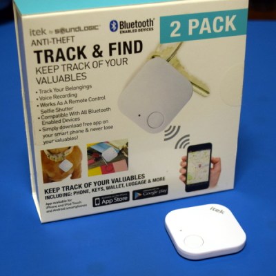 Which is precisely how I came to purchase a two pack of Bluetooth Low Energy (BLE) “trackers” for the princely sum of $10 USD. I didn’t expect much out of them for $5 each, but as this seemed an exceptionally low price for such technology in a brick and mortar store, I couldn’t resist. Plus there was something familiar about the look of the tracker that I couldn’t quite put my finger on while I was still in the store.
That vague feeling of recollection sent me digging through my parts bin as soon as I got home, convinced that I had seen something among the detritus that reminded me of my latest prize. Sure enough, I found a “Cube” Bluetooth tracker which, ironically, I had received as a Christmas gift some years ago. Putting them side by side, it was clear that the design of these “itek” trackers took more than a little inspiration from the better known (and five times as expensive) product.
The Cube was a bit thicker, but otherwise the shape, size, and even button placement on the itek was nearly identical. Reading through their respective manuals, the capabilities also seemed in perfect parity, down to being able to use the button on the device as a remote camera control for your smartphone. Which got me thinking: just how similar would these two devices be internally? Clearly they looked and functioned the same, but would they be built the same as well? They would have to cut costs somewhere.
Determined to find out how a company can put out what for all the world looks like a mirror image of a competitor’s device while undercutting them by such a large margin, I cracked both trackers open to get a bit more familiar with what makes them tick. What I found on closer inspection of these two similar gadgets is perhaps best summarized by that age old cautionary adage: “Don’t judge a book by its cover.”
Continue reading “A Cloned Bluetooth Tracker Meets Its Maker” →