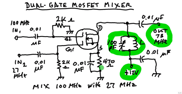
A mixer takes two signals and mixes them together. The resulting output is usually both frequencies, plus their sum and their difference. For example, if you feed a 5 MHz signal and a 20 MHz signal, you’d get outputs at 5 MHz, 15 MHz, 20 MHz, and 25 MHz. In a balanced mixer, the original frequencies cancel out, although not all mixers do that or, at least, don’t do it perfectly. [W1GV] has a video that explains the design of a mixer with a dual gate MOSFET, that you can see below.
The dual gate MOSFET is nearly ideal for this application with two separate gates that have effectively infinite input impedance. [Stan] takes you through the basic circuit and explains the operation in whiteboard fashion.
Using a MOSFET as a switch is generally pretty simple. Make the gate voltage sufficient with respect to the source and current flows through the channel. However, if you are switching higher voltages, you may need some additional circuitry to protect the device’s gate and possibly the microcontroller driving the whole thing, too. [Lewis] discusses high voltage switching in the latest in his series of videos dealing with MOSFETs. You can see the video below.
You’ll see in the video a breadboard setup driving a 50 V load and also a higher-voltage H-bridge. There are three major topics covered: Using an optoisolator, using a gate bleeder resistor, and using a zener diode to limit gate voltage.
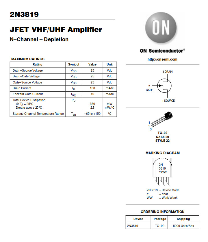
The 2N3819 is the archetypal general-purpose N-channel FET. (ON Semiconductor)
Over the recent weeks here at Hackaday, we’ve been taking a look at the humble transistor. In a series whose impetus came from a friend musing upon his students arriving with highly developed knowledge of microcontrollers but little of basic electronic circuitry, we’ve examined the bipolar transistor in all its configurations. It would however be improper to round off the series without also admitting that bipolar transistors are only part of the story. There is another family of transistors which have analogous circuit configurations to their bipolar cousins but work in a completely different way: the Field Effect Transistors, or FETs.
In a way it’s less pertinent to look at FETs in the way we did bipolar transistors, because while they are very interesting devices that power much of what you will do with electronics, you will encounter them as discrete components surprisingly rarely. Every CMOS device you deal with relies on FETs for its operation and every high-quality op-amp you throw a signal at will do so through a FET input, but these FETs are buried inside the chip and you’d be hard-pressed to know they were there if we hadn’t told you. You’d use a FET if you needed a high-impedance audio preamp or a low-noise RF amplifier, and FETs are a good choice for high-current switching applications, but sadly you will probably never have a pile of general-purpose FETs in the way you will their bipolar equivalents.
That said, the FET is a fascinating device. Join us as we take an in-depth look at their operation, and how and where you might use one.
FET basics
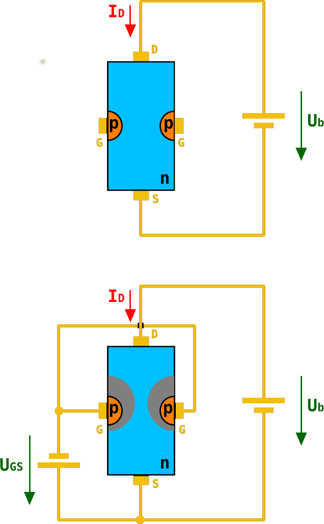
A diagram of an n-channel JFET. As the negative gate voltage on the p-type silicon decreases in the lower diagram, its electric field restricts the area through which electrons can flow in the n-type channel. Chtaube,(CC BY-SA 2.0 DE)
A basic FET has three terminals, a source (the source of electrons), a gate (the control terminal), and a drain (where electrons leave the device). These are analogous to the terminals on a bipolar transistor, in that the source fulfills a similar role to the emitter, the gate to the base, and the drain to the collector. Thus the three basic bipolar transistor circuit configurations have equivalents with a FET; common-emitter becomes common-source, common-base becomes common-gate, and an emitter follower becomes a source follower. It is dangerous to stretch the analogy between bipolar transistors and FETs too far, though, because of their different mode of operation. A closer similarity exists between a FET and a triode tube, if that helps.
The simplest FET for demonstration purposes has a piece of N-type semiconductor with source and drain connections at opposite ends, and a zone of P-type semiconductor deposited in its middle. This is referred to as an N-channel junction FET or JFET, because the channel through which current flows is N-type semiconductor, and because a diode junction exists between gate and channel. There are equivalent P-channel devices, just as there are PNP and NPN bipolar transistors.
Were you to bias an n-channel JFET as you would a bipolar transistor with a positive bias on its gate, the diode between gate and source would conduct, and the transistor would remain a diode with two cathode terminals. If however you give the gate a negative bias compared to the source, the diode becomes reverse-biased, and no current to speak of flows in the gate.
A characteristic of a reverse-biased diode is that it has a depletion zone between anode and cathode, an area in which there are no electrons. This is what causes the diode to no longer conduct, and the size of the depletion zone depends upon the size of the electric field that exists across it. If you’ve ever used a varicap diode, the capacitance between the two sides of this variable-width zone is the property you are exploiting.
In a FET, the depletion zone stretches from the gate region into the channel, and since its size can be adjusted by the gate voltage it can be used to “pinch” the remaining conductive region within the channel. Thus the area through which electrons can flow is controlled by the gate voltage, and thus the current that flows between drain and source is proportional to the gate voltage. We have an amplifier.
A simple FET radio receiver circuit showing FET biasing. The gate is biased at ground potential through the inductor, and the source is held above ground by the current in the 5K resistor. Herbertweidner [Public domain].In the JFET diagram above, the negative gate bias is represented by a battery. Tube enthusiasts may have encountered equipment that derives negative grid bias from a power supply, and you will find tube power units that include a -150 V rail for this purpose. In general though this is inconvenient in a FET circuit even though the voltage is lower, because of the extra cost of a negative regulator.. Instead the gate is held at a lower potential than the source by careful selection of a source resistor such that the current flowing through it brings the source up above ground, and a gate bias circuit that holds the gate close to ground. The base resistor chain from the bipolar circuit is for this reason often replaced with either a single resistor to ground, or a gate circuit with a very low DC resistance to ground such as an inductor.
MOSFETs, where the FET becomes more useful
Internal structure of an N-channel MOSFET. Fred the Oyster [Public domain].The JFET we have described is the simplest of field-effect devices, but it is not the one you will encounter most frequently. MOSFETs, short for Metal Oxide Semiconductor FETs, have a similar source, gate, and drain, but instead of relying on a depletion zone in a reverse-biased diode, they have a thin layer of insulation. The electric field from the gate acts across this insulation and pinches the conductive region in the channel through repulsion of electrons, with the same effect as it has in the JFET. It is beyond the scope of this piece to go into their mechanisms, but you will encounter two types of MOSFET: depletion mode devices that require the same negative bias as the JFET, and enhancement mode MOSFETS that require a positive bias.
Why would you use a FET?
So we’ve described the FET, and noted that while its mode of operation is different to that of a bipolar transistor it does a substantially similar job. Why would we use a FET then, what advantages does it offer us? The answer comes from the gate being insulated either by a depletion region in a JFET or by an insulating layer in a MOSFET. A FET is a voltage amplifier rather than a current amplifier, its input impedance is many orders higher than that of a bipolar transistor, and thus you will find FETs used in many applications that require a high impedance small-signal amplifier. The input of a high-performance op-amp will almost certainly be a FET, for example.
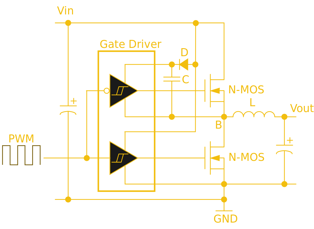
This half-bridge power MOSFET driver circuit uses a specialist gate driver IC with a pair of Schmidt buffers to deliver the initial surge required for a fast-turn-on time. Wdwd (CC BY 3.0).
The high input impedance has another effect less coupled to small signal work. Where a bipolar transistor requires significant base current to turn itself on, the corresponding FET requires almost none. Thus almost all complex integrated circuit logic devices are FET-based rather than bipolar because of the huge power saving that can be made by not needing to supply the base current demands of many thousands of bipolar transistors.
The same effect influences the choice of FETs for power switching, while a bipolar transistor’s base current is proportional to its collector current and thus it will need a significant driver, by contrast a power MOSFET requires virtually no standing gate current after an initial surge. A MOSFET power switch can thus be built requiring much less in the way of drive electronics and much more efficiently than a corresponding bipolar switch, and makes possible some of the tiny driver boards you might be used to for driving motors in your 3D printer, or your multirotor.
Through the course of this series you should have acquired a solid grounding in basic bipolar transistor principles, and now you should be able to add FETs to that knowledge base. We suggested you buy a bag of 2N3904s to experiment with in one of the previous articles, can we now suggest you do the same with a bag of 2N3819s?
It never fails — we post a somewhat simple project using a microcontroller and someone points out that it could have been accomplished better with a 555 timer or discrete transistors or even a couple of vacuum tubes. We welcome the critiques, of course; after all, thoughtful feedback is the point of the comment section. Sometimes the anti-Arduino crowd has a point, but as [Great Scott!] demonstrates with this microcontroller-less boost converter, other times it just makes sense to code your way out of a problem.
Built mainly as a comeback to naysayers on his original boost-converter circuit, which relied on an ATtiny85, [Great Scott!] had to go to considerable lengths to recreate what he did with ease using a microcontroller. He started with a quick demo using a MOSFET driver and a PWM signal from a function generator, which does the job of boosting the voltage, but lacks the feedback needed to control for varying loads.
Ironically relying on a block diagram for a commercial boost controller chip, which is probably the “right” tool for the job he put together the final circuit from a largish handful of components. Two op amps form the oscillator, another is used as a differential amp to monitor the output voltage, and the last one is a used as a comparator to create the PWM signal to control the MOSFET. It works, to be sure, but at the cost of a lot of effort, expense, and perf board real estate. What’s worse, there’s no simple path to adding functionality, like there would be for a microcontroller-based design.
Of course there are circuits where microcontrollers make no sense, but [Great Scott!] makes a good case for boost converters not being one of them if you insist on DIYing. If you’re behind on the basics of DC-DC converters, fear not — we’ve covered that before.
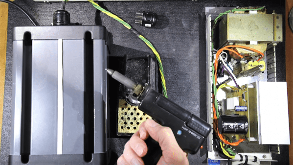
A dedicated desoldering station is a fantastic tool if you’re in the business of harvesting components from old gear. Having heat and suction in a single tool is far more convenient than futzing with spring-loaded solder suckers or braid, but only as long as the suction in the desoldering tool has a little oomph behind it. So if the suction on your solder sucker is starting to suck, this simple VFD can help restore performance.
Luckily for [Mr. Carlson], his Hakko 470 desoldering station is equipped with an AC induction motor, so it’s a perfect candidate for a variable frequency drive to boost performance. He decided to build a simple VFD that boosts the frequency from 60-Hz mains to about 90-Hz, thereby jacking the motor speed up by 50%. The VFD is just a TL494 PWM chip gating the primary coil of a power transformer through a MOSFET. Duty cycle and frequency are set by trimmers, and the whole thing is housed in an old chassis attached to the Hakko via an anachronistic socket and plug from the vacuum tube days. That’s a nice touch, though, because the Hakko can be returned to stock operation by a simple bridging plug, and the video below shows the marked difference in motor speed both with and without the VFD plugged in.
A classic one-man band generally features a stringed instrument or two, a harmonica in a hands-free holder, and some kind of percussion, usually a bass drum worn like a backpack and maybe some cymbals between the knees. The musician might also knock or tap the sound-boards of stringed instruments percussively with their strumming hand, which is something classical and flamenco guitarists can pull off with surprising range.
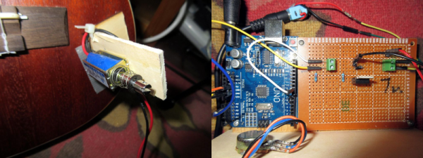
The musician usually has to manipulate each instrument manually. When it comes to percussion, [JimRD] has another idea: keep the beat by pounding the soundboard with a solenoid. He built a simple Arduino-driven MOSFET circuit to deliver knocks of variable BPM to the sound-board of a ukulele. A 10kΩ pot controls the meter and beat frequency, and the sound is picked up by a mic on the bridge. So far, it does 3/4 and 4/4 time, but [JimRD] has made the code freely available for expansion. Somebody make it do 5/4, because we’d love to hear [JimRD] play “Take Five“.
He didn’t do this to his good uke, mind you—it’s an old beater that he didn’t mind drilling and gluing. We were a bit skeptical at first, but the resonance sweetens the electromechanical knock of the solenoid slug. That, and [JimRD] has some pretty good chops. Ax your way past the break to give it a listen.
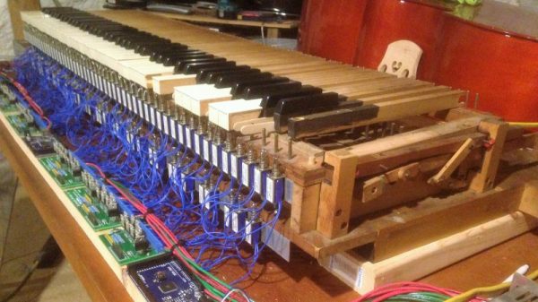
What did you do in high school? Chances are it wasn’t anywhere near as cool as turning a reed organ into a MIDI device. And even if you managed to pull something like that off, did you do it by mechanically controlling all 88 keys? Didn’t think so.
A reed organ is a keyboard instrument that channels moving air over sets of tuned brass reeds to produce notes. Most are fairly complex affairs with multiple keyboards and extra controls, but the one that [Willem Hillier] scored for free looks almost the same as a piano. Even with the free instrument [Willem] is about $500 into this project. Almost half of the budget went to the solenoids and driver MOSFETs — there’s a solenoid for each key, after all. And each one required minor surgery to reduce the clicking and clacking sounds that don’t exactly contribute to the musical experience. [Willem] designed custom driver boards for the MOSFETs with 16 channels per board, and added in a couple of power supplies to feed all those hungry solenoids and the three Arduinos needed to run the show. The video below shows the organ being stress-tested with the peppy “Flight of the Bumblebee”; there’s nothing wrong with a little showing off.

![A simple FET radio receiver circuit showing FET biasing. The gate is biased at ground potential through the inductor, and the source is held above ground by the current in the 5K resistor. Herbertweidner [Public domain].](https://hackaday.com/wp-content/uploads/2018/06/1kreiser_mit_fet.png)
![Internal structure of an N-channel MOSFET. Fred the Oyster [Public domain].](https://hackaday.com/wp-content/uploads/2018/04/n-channel_mosfet-svg1.png)