When it comes to getting retro hardware running again, there are many approaches. On one hand, the easiest path could be to emulate the hardware on something modern, using nothing but software to bring it back to life. On the other, many prefer to restore the original hardware itself and make sure everything is exactly as it was when it was new. A middle way exists, though, thanks to the widespread adoption of FPGAs which allow for programmable hardware emulation and [Jo] has come up with a new implementation of the Commodore 64 by taking this path.
The project is called the VIC64-T9K and is meant as a proof-of-concept that can run the Commodore 64’s VIC-II video chip alongside a 6502 CPU on the inexpensive Tang Nano 9k FPGA. Taking inspiration from the C64_MiSTer project, another FPGA implementation of the C64 based on the DE10-Nano FPGA, it doesn’t implement everything an original Commodore system would have had, but it does provide most of the core hardware needed to run a system. The project supports HDMI video with a custom kernel, and [Jo] has used it to get a few demos running including sprite animations.
Today we heard from [Richard James Howe] about his new CPU. This new 16-bit CPU is implemented in VHDL for an FPGA.
The really cool thing about this CPU is that it eschews the typical program counter (PC) and replaces it with a linear-feedback shift register (LFSR). Apparently an LFSR can be implemented in hardware with fewer transistors than are required by an adder.
Usually the program counter in your CPU increments by one, each time indicating the location of the next instruction to fetch and execute. When you replace your program counter with an LFSR it still does the same thing, indicating the next instruction to fetch and execute, but now those instructions are scattered pseudo-randomly throughout your address space!
Spade is an open-source hardware description language (HDL) developed at Linköping University, Sweden.
Other HDLs you might have heard of include Verilog and VHDL. Hardware engineers use HDLs to define hardware which can be rendered in silicon. Hardware defined in HDLs might look like software, but actually it’s not software, it’s hardware description. This hardware can be realized myriad ways including in an FPGA or with an ASIC.
You have probably heard that your CPU processes instructions in a pipeline. Spade has first-class support for such pipelines. This means that design activities such as re-timing and re-pipelining are much easier than in other HDLs where the designer has to implement these by hand. (Note: backward justification is NP-hard, we’re not sure how Spade supports this, if it does at all. If you know please enlighten us in the comments!)
Spade implements a type system for strong and static typing inspired by the Rust programming language and can do type inference. It supports pattern matching such as you might see in a typical functional programming language. It boasts having user-friendly and helpful error messages and tooling.
Spade is a work in progress so please expect missing features and breaking changes. The documentation is in The Spade Book. If you’re interested you can follow development on GitLab or Discord.
So now that you know about the Spade language, are you planning to take it for a spin? You will find plenty of Verilog/VHDL designs at Hackaday which you could re-implement using Spade, such as an easy one like Breathing LED Done With Raw Logic Synthesized From A Verilog Design (see benchmarks) or a much more challenging one like Game Boy Recreated In Verilog. If you give Spade a go we’d love to see what you come up with!
We’ve been fans of the Yosys / Nextpnr open-source FPGA toolchain for a long while now, and like [Michael] we had no idea that their oss-cad-suite installer sets up everything so that you can write in Verilog or VHDL, your choice. Very cool!
Verilog and VHDL are kind of like the C and ADA of the FPGA world. Verilog will seem familiar to you if you’re used to writing code for computers. For instance, it will turn integer variables into wires that carry the binary values for you. VHDL code looks odd from a software programmer’s perspective because it’s closer to the hardware and strongly typed: an 8-bit integer isn’t the same as eight wires in VHDL. VHDL is a bigger jump if you have software in your brain, but it’s also a lot closer to describing how the hardware actually works.
We learned Verilog, because it’s what Yosys supported. But thanks to GHDL, a VHDL analyzer and synthesizer, and the yosys-ghdl-plugin, you can write your logic in VHDL too. Does this put an end to the FPGA-language holy wars? Thanks, Yosys.
[Michael] points out that this isn’t really news, because the oss-cad-suite install has been doing this for a while now, but like him, it was news to us, and we thought we’d share it with you all.
Want to get started with FPGAs and the open-source toolchain? Our own [Al Williams] wrote up a nice FPGA Boot Camp series that’ll take you from bits to blinking in no time.
The last time we checked in with [Downtown Doug Brown], he had some cheap Altera USB Blaster clones that didn’t want to work under Linux. The trick at that time was to change the device’s 24 MHz clock to 12 MHz. This month, he’s found some different ones that don’t work, but now the clock change doesn’t work. What’s the problem?
He also picked up a Terasic clone, which does work on Linux and is considered, according to [Doug], the best of the clones. The units were superficially similar. So what follows is a lot of USB tracing and dumping of the CPLD chip’s configuration.
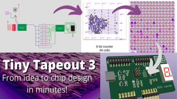
Custom semiconductor chips are generally big projects made by big companies with big budgets. Thanks to Tiny Tapeout, students, hobbyists, or anyone else can quickly get their designs onto an actual fabricated chip. [Matt Venn] has announced the opening of a third round of the Tiny Tapeout project for March 2023.
In 2022, Tiny Tapeout 1 piloted fabrication of user designs onto custom chips referred to as application-specific integrated circuits or ASICs. Following success of the pilot round, Tiny Tapeout 2 became the first paid version delivering guaranteed silicon. For Tiny Tapeout 2, there were 165 submissions. Most submissions were designed using a hardware description language such as Verilog or Amaranth, but ASICs can also be designed in the visual schematic capture tool Wokwi.
Each submitted design must fit within 150 by 170 microns. That footprint can accommodate around one thousand standard cells, which is certainly enough to explore a digital system of real interest. Examples from Tiny Tapeout 2 include digital neurons, FPGAs, and RISC-V processor cores.
Once the 250 designs are submitted, they’ll be combined into a large grid along with a controller. The controller will receive input signals and pump the inputs via a scan chain through the entire grid to each design. The results from each design continue through the scan chain to be output from the grid. Since all 250 designs will be combined on to one chip, each designer will receive everybody else’s design along with their own. This shared process opens a huge opportunity for experimentation.
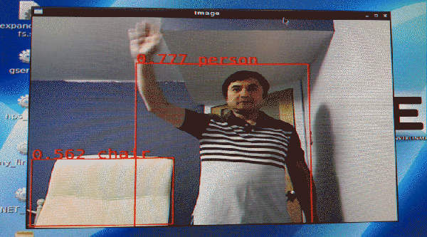
[Vuong Nguyen] clearly knows his way around artificial intelligence accelerator hardware, creating ztachip: an open source implementation of an accelerator platform for AI and traditional image processing workloads. Ztachip (pronounced “zeta-chip”) contains an array of custom processors, and is not tied to one particular architecture. Ztachip implements a new tensor programming paradigm that [Vuong] has created, which can accelerate TensorFlow tasks, but is not limited to that. In fact it can process TensorFlow in parallel with non-AI tasks, as the video below shows.
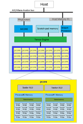
A RISC-V core, based on the VexRiscV design, is used as the host processor handling the distribution of the application. VexRiscV itself is quite interesting. Written in SpinalHDL (a Scala variant), it’s super configurable, producing a Verilog core, ready to drop into the design.
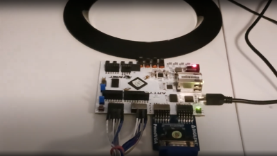
A Digilent Arty-A7, Arducam and a VGA PMOD is all you need
From a hardware design perspective the RISC-V core hooks up to an AXI crossbar, with all the AXI-lite busses muxed as is usual for the AMBA AXI ecosystem. The Ztachip core as well as a DDR3 controller are also connected, together with a camera interface and VGA video.
Other than providing an FPGA-specific DDR3 controller and AXI crossbar IP, the rest of the design is generic RTL. This is good news. The demo below deploys onto an Artix-7 based Digilent (Arty-A7) with a VGA PMOD module, but little else needed. Pre-build Xilinx IP is provided, but targeting a different FPGA shouldn’t be a huge task for the experienced FPGA ninja.
Ztachip top level architecture
The magic happens in the Ztachip core, which is mostly an array of Pcores. Each Pcore has both vector and scalar processing capability, making it super flexible. The Tensor Engine (internally this is the ‘dataplane processor’) is in charge here, sending instructions from the RISC-V core into the Pcore array together with image data, as well as streaming video data out. That camera is only a 0.3 MP Arducam, and the video is VGA resolution, but give it a bigger FPGA and those limits could be raised.
This domain-specific approach uses a highly modified C-like language (with a custom compiler) to describe the application that is to be distributed across the accelerator array. We couldn’t find any documentation on this, but there are a few example algorithms.
The demo video shows a real-time mix of four algorithms running in parallel; one object classification (Google’s Tensorflow mobilenet-ssd, a pre-trained AI model) canny edge detection, a Harris corner detection, and Optical flow which gives it a predator-like motion vision.
[Vuong] reckons, efficiency wise it is 5.5x more computationally efficient than a Jetson Nano and 37x more than Google’s TPU edge. These are bold claims, to say the least, but who are we to argue with a clearly incredibly talented engineer?