High-Tech Paperweight Shows Off Working 60s-era Thin-Film Electronics

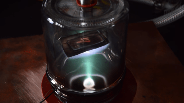
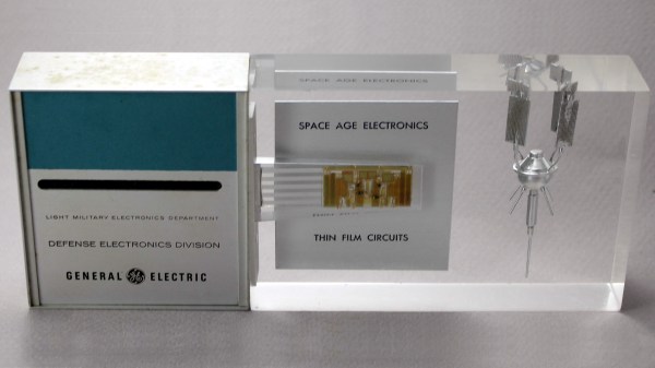
[Ken Shirriff]’s analysis of a fascinating high-tech paperweight created by GE at the height of the space race is as informative as it is fun to look at. This device was created to show off GE’s thin-film electronics technology, and while it’s attractive enough on its own, there’s an added feature: as soon as the paperweight is picked up, it begins emitting a satellite-like rhythmic beep. It is very well-made, and was doubtlessly an impressive novelty for its time. As usual, [Ken] dives into what exactly makes it tick, and shares important history along the way.

Thin-film module with labels, thanks to [Ken]’s vintage electronics detective work. Click to enlarge.
In the clear area of the paperweight is a thin-film circuit, accompanied by a model of an early satellite. The module implements a flip-flop, and the flat conductors connect it to some additional components inside the compartment on the left, which contains a power supply and the necessary parts to create the beeps when it is picked up.

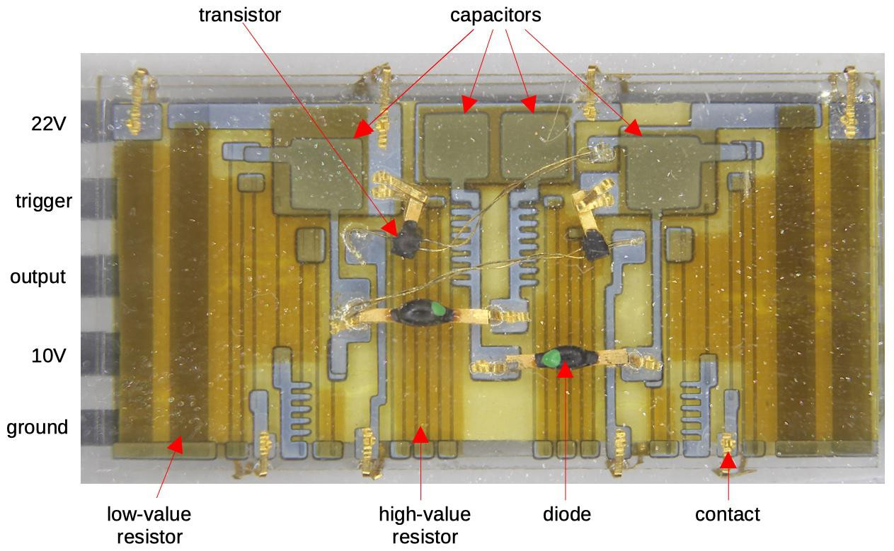
Thin-film electronics reduced the need for individual components by depositing material onto a substrate to form things like resistors and capacitors. The resulting weight and space savings could be considerable, and close-ups of the thin film module sure look like a precursor to integrated circuits. The inside of the left compartment contains a tilt switch, a battery, a vintage earphone acting as a small speaker, and a small block of components connected to the thin-film module. This block contains two oscillators made with unijunction transistors (UJTs); one to create the beep, and one to control each beep’s duration. The construction and overall design of the device is easily recognizable, although some of the parts are now obsolete.

If you’d like a bit more detail on exactly how this device worked, including circuit diagrams and historical context, be sure to click that first link, and pay attention to the notes and references at the end. One other thing that’s clear is that functional electronics embedded in clear plastic shapes simply never go out of style.

Vacuum Sputtering With A Homemade Magnetron

“You can never be too rich or too thin,” the saying goes, and when it comes to coatings, it’s true that thinner is often better. The way to truly thin coatings, ones that are sometimes only a few atoms thick, is physical vapor deposition, or PVD, a technique where a substance is transformed into a vapor and condensed onto a substrate, sometimes using a magnetron to create a plasma.

It sounds complicated, but with a few reasonable tools and a healthy respect for high voltages, a DIY magnetron for plasma sputtering can get you started. To be fair, [Justin Atkin] worked on his setup for years, hampered initially by having to settle for found parts and general scrap for his builds. As with many things, access to a lathe and the skills to use it proved to be enabling, allowing him to make custom parts like the feedthrough for the vacuum chamber as well as a liquid-cooled base, which prevents heat from ruining the magnets that concentrate the plasma onto the target metal. Using a high-voltage DC supply made from old microwave parts, [Justin] has been able to sputter copper films onto glass slides, with limited success using other metals. He also accidentally created a couple of dichroic mirrors by sputtering with copper oxides rather than pure copper. The video below has some beautiful shots of the ghostly green and purple glow.

A rig such as this opens up a lot of possibilities, from optics to DIY semiconductors. It may not be quite as elaborate as some PVD setups we’ve seen, but we’re still pretty impressed.

Continue reading “Vacuum Sputtering With A Homemade Magnetron”

Julius Lilienfeld And The First Transistor

Here’s a fun exercise: take a list of the 20th century’s inventions and innovations in electronics, communications, and computing. Make sure you include everything, especially the stuff we take for granted. Now, cross off everything that can’t trace its roots back to the AT&T Corporation’s research arm, the Bell Laboratories. We’d wager heavily that the list would still contain almost everything that built the electronics age: microwave communications, data networks, cellular telephone, solar cells, Unix, and, of course, the transistor.

But is that last one really true? We all know the story of Bardeen, Brattain, and Shockley, the brilliant team laboring through a blizzard in 1947 to breathe life into a scrap of germanium and wires, finally unleashing the transistor upon the world for Christmas, a gift to usher us into the age of solid state electronics. It’s not so simple, though. The quest for a replacement for the vacuum tube for switching and amplification goes back to the lab of  Julius Lilienfeld, the man who conceived the first field-effect transistor in the mid-1920s.

Continue reading “Julius Lilienfeld And The First Transistor”

Of Roach Killer And Rust Remover: Sam Zeloof’s Garage-Made Chips

A normal life in hacking, if there is such a thing, seems to follow a predictable trajectory, at least in terms of the physical space it occupies. We generally start small, working on a few simple projects on the kitchen table, or if we start young enough, perhaps on a desk in our childhood bedroom. Time passes, our skills increase, and with them the need for space. Soon we’re claiming an unused room or a corner of the basement. Skills build on skills, gear accumulates, and before you know it, the garage is no longer a place for cars but a place for pushing back the darkness of our own ignorance and expanding our horizons into parts unknown.

It appears that Sam Zeloof’s annexation of the family garage occurred fairly early in life, and to a level that’s hard to comprehend. Sam seems to have caught the hacking bug early, and by the time high school rolled around, he was building out a remarkably well-equipped semiconductor fabrication lab at home. Sam has been posting his progress regularly on his own blog and on Twitter, and he dropped by the 2018 Superconference to give everyone a lesson on semiconductor physics and how he became the first hobbyist to produce an integrated circuit using lithographic processes.

Continue reading “Of Roach Killer And Rust Remover: Sam Zeloof’s Garage-Made Chips”

Tiny Vacuum Chamber Arm To Help With Homemade Semiconductors

[Nixie] wants to make semiconductors at home, and that requires some unusual tools. Chief among them is a vacuum chamber to perform thin-film deposition, and true to the hacker credo his is homemade, and will soon be equipped with a tiny manipulator arm with magnetically coupled mechanical controls.

If [Nixie]’s setup looks familiar, it might be because we featured his plasma experiments a few days ago. He was a little cagey then about his goal, but he’s come clean with his desire to make his own FETs (a project that is his 2018 Hackaday Prize entry). Doing so will require not only creating stable plasmas, but also the ability to move substrates around inside the vacuum chamber. Taking inspiration from the slender and maneuverable instruments surgeons use for laparoscopic procedures, [Nixie] is working on a miniature arm that will work inside his vacuum chamber. The video below is a 3D-printed proof-of-concept model in action, and shows how the arm’s segments will be controlled by cables. What’s really interesting is that the control cables will not penetrate the vacuum chamber — they’ll be moved right through the glass wall using magnets.

We’re keen to see chips from [Nixie]’s home fab lab, but it looks like there will be a lot of cool hacks between here and there. We’ll be watching closely. Continue reading “Tiny Vacuum Chamber Arm To Help With Homemade Semiconductors”

Home Brew Solar Cells For The Chemically Curious

The idea of making your own semiconductors from scratch would be more attractive if it weren’t for the expensive equipment and noxious chemicals required for silicon fabrication. But simple semiconductors can be cooked up at home without anything fancy, and they can actually yield pretty good results.

Granted, [Simplifier] has been working on the method detailed in the video below for about a year, and a look at his post on copper oxide thin-film solar cells reveals a meticulous approach to optimize everything. He started with regular window glass, heated over a propane burner and sprayed with a tin oxide solution to make it conductive while remaining transparent. The N-type layer was sprayed on next in the form of zinc oxide doped with magnesium. Copper oxide, the P-type layer, was electroplated on next, followed by a quick dip in copper sulfide to act as another transparent conductor. A conductive compound of sodium silicate and graphite was layered on the back to form the electrical contacts. The cell worked pretty well — 525 mV open circuit voltage and 6.5 mA short-circuit current. Not bad for home brewed.

If you want to replicate [Simplifier]’s methods, you’ll find his ample documentation of his site. Of course, if you yearn for DIY silicon semiconductors, there’s a fab for that, too.

Continue reading “Home Brew Solar Cells For The Chemically Curious”

Adventures With Vacuum Deposition Power Supplies

[macona] called this a “fail of the week”, but of course failure is just another part of the hacker adventure. Fail and fail often! He’s been slowly assembling a vacuum deposition system. These systems let you deposit thin films on a substrate. Vacuum deposition systems have all sorts of exciting applications, not only are they used in semiconductor manufacturing, but as [Ben Krasnow] has shown can create conductive transparent coatings. They’re even sometimes used for silvering mirrors.

A common feature of these systems is that they require high voltage, we’re not talking a few hundred volts or even a few thousand volts. But 10 to 20 kilovolts. You need such a high voltage in order to accelerate electrons and ions, which are used to eject atoms from a source and deposit them as a thin film on a substrate.

It was this HV supply [macona] was working on, cobbling the system together from parts found on eBay. Unfortunately he could only reach 9kv unloaded, which we’d expect to drop considerably under load. So [macona] has now found a different solution. But this teardown and write up still makes great reading.

We’re left to pondering on what projects the spare parts could be useful for: “I might be able to series the secondaries and get 30kv at 500ma! That would make one hell of a bug zapper! Actually these transformers scare the hell out of me….” me too Jerry! Me too!