[Kenneth Wilke] is undertaking a noble quest – to build a homebrew microcomputer, based around the venerable 6502. As a prelude to this, he set out to interface the hallowed CPU to an FPGA, and shared the process involved.
[Kenneth] is using an Arty A7 FPGA development board which is a great fit for purpose, having plenty of I/O pins and being relatively easy to work with for the home tinkerer. This is an important consideration, as many industrial strength FPGAs require software licences to use which can easily stretch into the tens of thousands of dollars.
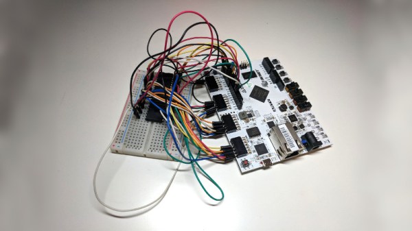
The 6502 is placed on a breadboard, and a nest of wires connects it to the PMOD interfaces of the Arty board. Then it’s a simple job of mapping out the pins on the FPGA and you’re good to go. Due to the 6502’s design it’s possible to step through instructions one at a time, and this is particularly useful on a basic homebrew build so [Kenneth] was sure to implement this functionality.
It’s all capped off with the FPGA sending the 6502 a starting address and a series of NOPs, to demonstrate the setup is capable of running the 6502 with instructions fed from the FPGA. It’s a project that shows the fundamentals of interfacing two technologies that are widely spread out in sophistication, and acts as a great base for further experimentation.
We can’t wait to see what [Kenneth] does next, as we’ve seen great things before.