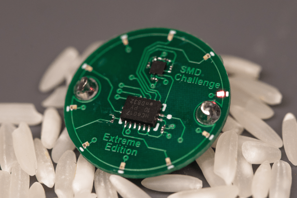
DIY Relay Module Saves Time

As any programmer could tell you, there’s significant value in automating a process that is performed often enough. The more times that process is used, the more it makes sense to automate it or at least improve its efficiency. This rule isn’t limited to software though; improvements to hardware design can also see improvements in efficiency as well. For that reason, [Hulk] designed a simple relay module in order to cut the amount of time he spends implementing this solution in his various other projects.

While driving a relay with a transistor is something fundamental, this project isn’t really about that per se. It’s about recognizing something that you do too much, and then designing that drudgery out of your projects. [Hulk] was able to design a PCB with 12 modules on it, presumably saving fabrication costs. He can then easily populate them with specific components as soon as he needs one. Another benefit of designing something like this yourself, rather than an off-the-shelf relay module, is that you can do away with any useless features you’ll never need (or add ones that aren’t available in commercial devices).

We can appreciate the efficiency gains this would make for our next project that needs a simple driver for a light, garage door opener, or any other binary electronic device. It can be a hassle to go find the correct transistor and relay, solder it all on the project board, and hope it all works. A pre-made solution solves all these issues, but we do wish the schematics were available to keep us from having to design our own. Driver boards are a pretty common project for all the different types of relays we see around here, so there is probably one available out there.

Perfect Photographs For PCB Reverse Engineering

There’s an unexpected part of hacking that is very difficult to get right, namely photographing printed circuit boards. Everything seems to catch the light, making for a complex dance of manipulating light sources and camera angles. We were thus captured by [Roman Valls]’ budget rig for taking PCB photos that makes ingenious use of roadside trash to achieve a result.

It was inspired by a video featuring a much more accomplished rig, which he set out to emulate for much less outlay. Instead of an expensive lens, he’s using a Nikon camera with its kit lens. And instead of a tripod there’a a scrap drawer salvaged from the roadside and modified to become a camera holder. Lighting is diffused by baking paper, and the result is a rig that can photograph PCBs with neutral lighting and without annoying highlights.

We especially like work that takes junk and makes something useful from it, and though our purpose isn’t in reverse engineering it’s impressive to see how well the technique reveals the traces. We’ll definitely be experimenting with some of the techniques herein, and those lighting tips might also work with the Hackaday ear camera microscope.

An Analog IC Design Book Draft

[Jean-Francois Debroux] spent 35 years designing analog ASICs. He’s started a book and while it isn’t finished — indeed he says it may never be — the 180 pages he posted on LinkedIn are a pretty good read.

The 46 sections are well organized, although some are placeholders. There are sections on design flow and the technical aspects of design. Examples range from a square root circuit to a sigma-delta modulator, although some of them are not complete yet. There are also sections on math, physics, common electronics, materials, and tools.

Continue reading “An Analog IC Design Book Draft”

Transparent OLED Hitting The Market With Xiaomi’s Mi TV LUX Transparent Edition

One of the major advantages of OLED over LCD panels is that the former can be made using far fewer layers as the pixels themselves are emitting the light instead of manipulating the light from a backlight. This led some to ask the question of whether it’s possible to make an OLED panel that is transparent or at least translucent. As Xiaomi’s new Mi TV LUX OLED Transparent Edition shows, the answer there is a resounding ‘yes’. Better yet, for a low-low price of about $7,200 you can own one of these 55″ marvels.

Transparent OLED technology is not new, of course. Back in 2018 LG was showing off a prototype TV that used one of the early transparent OLED panels. In the video that is embedded after the break, [Linus] from Linus Tech Tips goes hands-on with that LG prototype while at LG in South Korea, while including a number of crucial details from an interview from one of the engineers behind that panel.

As it turns out, merely removing the opaque backing from an OLED panel isn’t enough to make it transparent. In order for an OLED panel to become transparent, the circuitry in the pixel layer and TFT layer need to be aligned as best as possible to allow for many, many tiny holes to be punched through the display.

Looking at [Linus]’s experiences with the LG prototype, it does appear that this kind of technology would be highly suitable for signage purposes, while also allowing for something like an invisible television or display in a room that could be placed in front of a painting or other decoration. Once displaying an image, the screen is bright enough that you can comfortably make out the image. Just don’t put any bright lights behind the TV.

Anyone else anxious waiting for sub-10″ versions of these panels?

Continue reading “Transparent OLED Hitting The Market With Xiaomi’s Mi TV LUX Transparent Edition”

Want To Support Hacker-friendly Hardware Design? Follow Valve’s Example

It’s been just over a year since Valve released Index, their flagship VR system, and it’s worth looking back at this GitHub repository as a fine example of how to provide supporting materials to a hacker-friendly hardware design. The image above shows off one of the hacker-friendly design elements: an empty space behind the visor, with a USB port off to the right, that exists for no reason other than to make it easier to mount and plug in whatever one might come up with. There’s more to it than that, however. If one wishes to provide supporting materials for a hardware design, one could certainly do worse than emulate Valve’s example.

The violet 3D model shows the area that modifications can occupy without getting in the way of any sensors.

The hardware repository contains not just CAD models of mod-friendly hardware pieces (both in high-resolution STEP models as well as STL files) but also 3D models of the sensor zones, so modders can ensure they avoid occluding any sensors with their creations. Examples are great, and one provided by Valve is the Booster; a hand controller add-on providing extra comfort for people with large hands or long thumbs. The model also doubles as a reference for designing attachments that will not interfere with any of the tracking or touch-sensitive surfaces of the controllers.

Being hacker-friendly doesn’t mean the hardware has no warranty, but it does mean that there is concrete guidance on what does or doesn’t risk voiding it. In the case of the Index hardware, the guidance is simple: “Anything that requires a T5 or smaller is not user serviceable.”

To us, the whole attitude of being hacker-friendly is exemplified by a statement about the headstrap, found about half-way down the page. The words “removing the headstrap is not recommended” are followed immediately by clear directions on how to do exactly that, demonstrating the kind of trust necessary to reduce barriers for add-ons and modifications. That is a great way to help foster experimentation, like this project for 1:1 mapping of physical elements to their VR counterparts, to make awesome spaceship cockpits.

3D Printable Kinematic Couplings, Ready To Use

Time may bring change, but kinematic couplings don’t. This handy kinematic couplings resource by [nickw] was for a design contest a few years ago, but what’s great is that it includes ready-to-use models intended for 3D printing, complete with a bill of materials (and McMaster-Carr part numbers) for hardware. The short document is well written and illustrated with assembly diagrams and concise, practical theory. The accompanying 3D models are ready to be copied and pasted anywhere one might find them useful.

What are kinematic couplings? They are a way to ensure that two parts physically connect, detach, and re-connect in a precise and repeatable way. The download has ready-to-use designs for both a Kelvin and Maxwell system kinematic coupling, and a more advanced design for an optomechanical mount like one would find in a laser system.

The download from Pinshape requires a free account, but the models and document are licensed under CC – Attribution and ready to use in designs (so long as the attribution part of the license is satisfied, of course.) Embedded below is a short video demonstrating the coupling using the Maxwell system. The Kelvin system is similar.

Continue reading “3D Printable Kinematic Couplings, Ready To Use”

Hands-On: Internet Of Batteries Quantum Badge Brings Badgelife Add-Ons The Power And Internet They Crave

Our friends in the Whiskey Pirates crew sent me the unofficial DEF CON badge they built this year. The Internet of Batteries QUANTUM provides power and connectivity to the all-important add-on badges of DC28. The front of the badge is absolutely gorgeous to the point I don’t really want to solder on my add-on headers and disrupt that aesthetic.

The gold-plated copper makes for a uniformed and reflective contrast to the red solder mask which occupies the majority of the front. Here we see the great attention to detail that [TrueControl] includes in his badges. The white stripe of silk screen separating the two colors is covered by some black detailing tape that looks much better than the white.

The antenna of the ESP32 module poking out the underside of the gold cover end of the badge gets its own rectangle of the holographic sticker material, the same as the sheet of stickers that was included in the box. Both decals are small details that make a huge difference to your eye.

The line of nine RGB LEDs have black bezels which goes along with the black stripe motif and underscores the typography of the badge name. These lights are hosted on a daughter board soldered to the underside of the badge with a slot for the LEDs to pass through. They are addressed in a 2×15 matrix that is scanned on the low side by the PSoC5 that drives the badge. This low-res image shows that daughter board before the lithium cell is placed.

Continue reading “Hands-On: Internet Of Batteries Quantum Badge Brings Badgelife Add-Ons The Power And Internet They Crave”