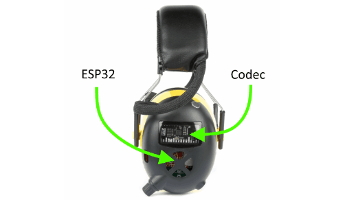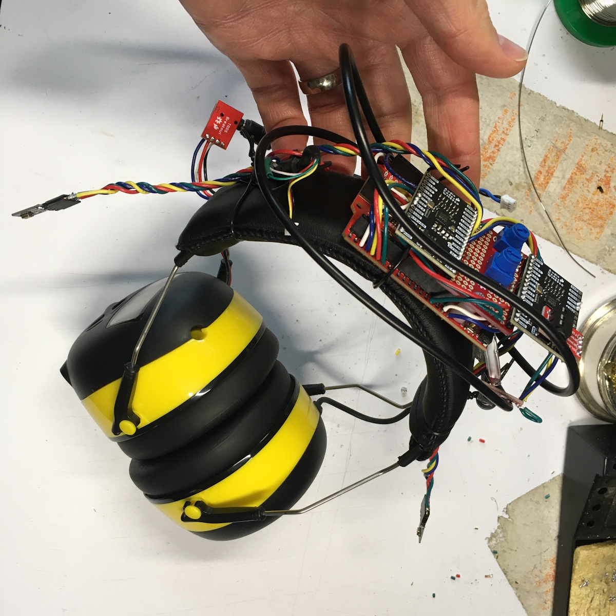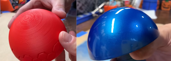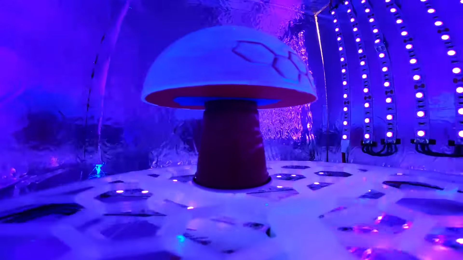
Even though it seems the worst of COVID has passed, October generally kicks off cold and flu season, so why not continue to pass out Halloween treats in a socially-distanced fashion?
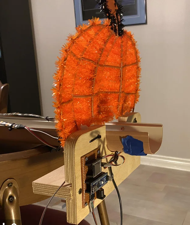 That is, of course the idea behind [Gord Payne]’s Halloween Treat Trough of Terror. Lay a treat at the top of the trough and it will activate the LED strips that follow the treat down to the end, as well as some spooky sounds. The treat in question is detected by an SR-04 ultrasonic distance sensor connected to an Arduino Nano.
All in all this was a highly successful build as far as neighborhood entertainment value goes. Toddlers stared in awe at the blinkenlights, teenagers proclaimed it ‘sick’, and we can only assume that the adults were likely happy to see something aimed at kids that’s not scary.
[Gord] has a nice how-to if you want to build your own, and of course, the Arduino sketch is available. Be sure to check it out in action after the break.
Don’t have room to build a treat slide? Here’s a socially-distanced dispenser that lets them stomp a giant button.
Continue reading “2023 Halloween Hackfest: Treat Trough Of Terror Is Actually Pretty Cute”