LTSpice and the underlying Spice engine does a great job of simulating ideal components. But it is also capable — if you know how — of handling models of real-world devices. Inductors, for example, are one of the most imperfect components. Their constituent wire has resistance, and there is parasitic capacitance between the windings. If there is a core, it also will have many imperfections and losses. [Sam Ben-Yaakov] has a lecture about modeling real inductors in LTSpice, and he covers how you can capture some of these imperfections in the video below.
There is a bit of math in the presentation, but we liked that it relates back to datasheets for actual components. Being able to understand what the parameters on a datasheet mean is crucial, and if you ever wondered what some of these entries mean, you’ll get a lot from this video.
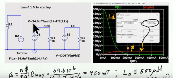
The main feature of the model is the flux equation. The tanh (hyperbolic tangent) function is similar to the curve you want for the flux equation, so it plays a major part. Of course, there are other parts of the inductor you may have to model, too, but this is one of the most difficult parts.
You can also model transformers using LTSpice. You can also create custom components.