Opening Up ASIC Design

The odds are that if you’ve heard about application-specific integrated circuits (ASICs) at all, it’s in the context of cryptocurrency mining. For some currencies, the only way to efficiently mine them anymore is to build computers so single-purposed they can’t do anything else. But an ASIC is a handy tool to develop for plenty of embedded applications where efficiency is a key design goal. Building integrated circuits isn’t particularly straightforward or open, though, so you’ll need some tools to develop them such as OpenRAM.

Designing the working memory of a purpose-built computing system is a surprisingly complex task which OpenRAM seeks to demystify a bit. Built in Python, it can help a designer handle routing models, power modeling, timing, and plenty of other considerations when building static RAM modules within integrated circuits. Other tools for taking care of this step of IC design are proprietary, so this is one step on the way to a completely open toolchain that anyone can use to start building their own ASIC.

This tool is relatively new and while we mentioned it briefly in an article back in February, it’s worth taking a look at for anyone who needs more than something like an FPGA might offer and who also wants to use an open-source tool. Be sure to take a look at the project’s GitHub page for more detailed information as well. There are open-source toolchains if you plan on sticking with your FPGA of choice, though.

Tiny Tapeout 3

Tiny Tapeout 3: Get Your Own Chip Design To A Fab

Custom semiconductor chips are generally big projects made by big companies with big budgets. Thanks to Tiny Tapeout, students, hobbyists, or anyone else can quickly get their designs onto an actual fabricated chip. [Matt Venn] has announced the opening of a third round of the Tiny Tapeout project for March 2023.

In 2022, Tiny Tapeout 1 piloted fabrication of user designs onto custom chips referred to as application-specific integrated circuits or ASICs. Following success of the pilot round, Tiny Tapeout 2 became the first paid version delivering guaranteed silicon. For Tiny Tapeout 2, there were 165 submissions. Most submissions were designed using a hardware description language such as Verilog or Amaranth, but ASICs can also be designed in the visual schematic capture tool Wokwi.

Each submitted design must fit within 150 by 170 microns. That footprint can accommodate around one thousand standard cells, which is certainly enough to explore a digital system of real interest.  Examples from Tiny Tapeout 2 include digital neurons, FPGAs, and RISC-V processor cores.

Once the 250 designs are submitted, they’ll be combined into a large grid along with a controller. The controller will receive input signals and pump the inputs via a scan chain through the entire grid to each design. The results from each design continue through the scan chain to be output from the grid. Since all 250 designs will be combined on to one chip, each designer will receive everybody else’s design along with their own. This shared process opens a huge opportunity for experimentation.

To get started on your own ASIC design right away, visit Tiny Tapeout. Also check out the talk [Matt] gave at Supercon 2022: Bringing Chip Design to the Masses along with his Zero to ASIC videos. And we’re not saying anything official, but he’ll probably be giving a workshop at Hackaday Berlin.

Continue reading “Tiny Tapeout 3: Get Your Own Chip Design To A Fab”

Matt Venn speaking at Supercon 2022

Supercon 2022: Matt Venn’s Tiny Tapeout Brings Chip Design To The Masses

Not that long ago, rolling your own printed circuit boards was difficult, time-consuming and expensive. But thanks to an army of cheap, online manufacturing services as well as high-quality free design software, any hobbyist can now make boards to rival those made by pros. A similar shift might be underway when it comes to chip design: affordable manufacturing options and a set of free software tools are slowly bringing custom chips into the realm of hackers and hobbyists. One of those working hard to democratize chip design is Matt Venn, who’s been telling us all about his current big project, called Tiny Tapeout, in his talk at Remoticon 2022.

Matt’s quest to bring IC design to the masses started in 2020, when the first open-source compatible Process Design Kit (PDK) was released to the public. A PDK is a collection of files, normally only available under strict non-disclosure agreements, that describe all the features of a specific chip manufacturing process and enable you to make a design. With this free PDK in hand and a rag-tag collection of free software tools, Matt set out to design his first chip, a VGA clock, which he taped out (released to manufacturing) in July 2020. Continue reading “Supercon 2022: Matt Venn’s Tiny Tapeout Brings Chip Design To The Masses”

It’s Not Easy Counting Transistors In The 8086 Processor

For any given processor it’s generally easy to find a statistic on the number of transistors used to construct it, with the famous Intel 8086 CPU generally said to contain 29,000 transistors. This is where [Ken Shirriff] ran into an issue when he sat down one day and started counting individual transistors in die shots of this processor. To his dismay, he came to a total of 19,618, meaning that 9,382 transistors are somehow unaccounted for. What is going on here?

The first point here is that the given number includes so-called ‘potential transistors’. Within a section of read-only memory (ROM), a ‘0’ would be a missing transistor, but depending on the programming of the mask ROM (e.g. for microcode as with a CISC x86 CPU), there can  be a transistor there. When adding up the potential but vacant transistor locations in ROM and PLA (programmable logic array) sections, the final count came to 29,277 potential transistors. This is much closer to the no doubt nicely rounded number of 29,000 that is generally used.

[Ken] also notes that further complications here are features such as driver transistors that are commonly found near bond wire pads. In order to increase the current that can be provided or sunk by a pad, multiple transistors can be grouped together to form a singular driver as in the above image. Meanwhile yet other transistors are used as (input protection) diodes or even resistors. All of which makes the transistor count along with the process node used useful primarily as indication for the physical size and complexity of a processor.

A sequence of pictures with arrows between each other. This picture shows a Wokwi (Fritzing-like) diagram with logic gates, going to a chip shot, going to a panel of chipsGA footprint on a KiCad PCB render with DIP switches and LEDs around the breakout. Under the sequence, it says: "Tiny Tapeout! Demystifying microchip design and manufacture"

Design Your Own Chip With TinyTapeout

When hackers found and developed ways to order PCBs on the cheap, it revolutionized the way we create. Accessible 3D printing brought us entire new areas to create things. [Matt Venn] is one of the people at the forefront of hackers designing our own silicon, and we’ve covered plenty of his research over the years. His latest effort to involve the hacker community, TinyTapeout, makes chip design accessible to newcomers – the bar is as low as arranging logic gates on a web browser page.

Six chip shots shown, with various densities of gates being used - some use a little, and some use a the entire area given.
Just six of the designs submitted, with varying complexity

For this, [Matt] worked with people like [Uri Shaked] of Wokwi fame, [Sylvain “tnt” Munaut], [jix], and a few others. Together, they created all the tooling necessary, and most importantly, a pipeline where your logic gate-based design in Wokwi gets compiled into a block ready to be put into silicon, with even simulations and compile-time verification for common mistakes. As a result, the design process is remarkably straightforward, to the point where a 9-year-old kid can do it. If you wanted, you could submit your Verilog, too!

The first round of TinyTapeout had a deadline in the first days of September and brought 152 entries together – just in time for an Efabless shuttle submission. All of these designs were put on a single instance of a chip, that will be fabbed in quantity, tested, soldered onto breakouts, and mailed out to individual participants. In this way, everyone will be getting everyone’s design, but thanks to the on-chip muxing hardware, they’re able to switch between designs using on-breakout DIP switches.

More after the break…

Continue reading “Design Your Own Chip With TinyTapeout”

The Open Source ASICs Hack Chat Redefines Possible

There was a time when all that was available to the electronics hobbyist were passive components and vacuum tubes. Then along comes the integrated circuit, and it changed everything. Fast forward a bit, and affordable programmable microcontrollers arrived on the scene. Getting started in electronics became far easier, and the line between hardware and software started to blur. Much more recently, the hobbyist community was introduced to field programmable gate arrays (FPGAs) and the tools necessary to work with them. While not as widely applicable as the IC or MCU, the proliferation of FPGAs among hardware hackers once again opened doors that were previously locked tight.

We’re currently on the edge of another paradigm shift, but it’s no surprise if you haven’t heard of it. After all, the last couple of years have been a bit unusual, so the 2020 announcement that Google was teaming up with SkyWater and Efabless to enable the design and manufacture of open source application-specific integrated circuits (ASICs) flew under the radar for many people. But not Matt Venn, the host of this week’s Hack Chat. For him, it was the opportunity he’d been waiting for.

Matt started like many of us, building electronic kits and building new gadgets out of old discarded hardware. He graduated to microcontrollers, and became particularly interested in FPGAs when the open source toolchains started hitting the scene. Of course by this point, it was much more than just a hobby for him. He was presenting a talk at the 2019 Week of Open Source Hardware in Switzerland when he saw Tim Edwards from Efabless demo a chip that had been made with open source tools. Unfortunately, the costs involved were still far too high for an individual to put their ideas into silicon.

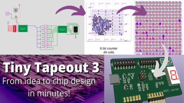
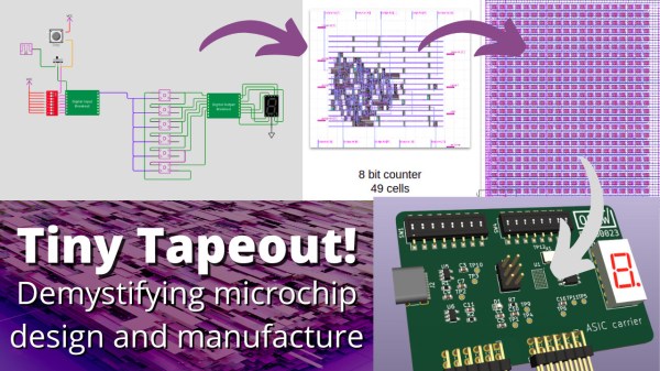
So when Google and Skywater announced they would be footing the bill to have selected open source ASIC designs manufactured a few months later, Matt says he was in a good position to jump in. He has since started running the Zero to ASIC Course which aims to teach you how to produce your own chips using the open source Process Development Kit, and so far 160 people have taken him up on the offer.

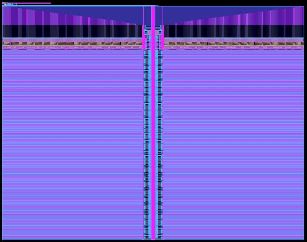
As you might expect, many of the questions in the Chat had to do with what kind of designs you can actually produce using the 130 nm process. Especially given the limits on the physical space each creator’s circuit can take up on each multi-project wafer (MPW). Others wanted to know how difficult it would be to port over existing FPGA designs, or how well the process worked with analog applications. With the number of designs Matt has seen go through his course, he could answer many of the questions just by pointing to a particular individual’s ASIC. For instance, he held up the digital-to-analog converter from Harald Pretl and Thomas Parry’s 5 GHz satellite transceiver as prime analog examples.

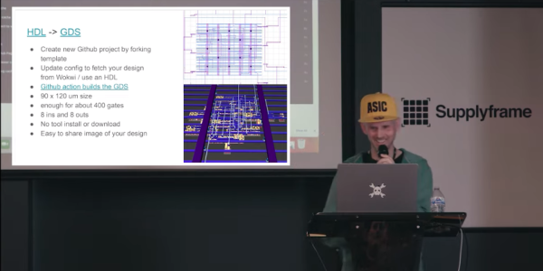
So let’s say you put the work in to design an ASIC and it gets approved to be produced on a future MPW, what then? Well, first you have to hope everything goes according to plan. Matt explains that the initial run was almost a total write-off due to timing problems in the toolchain, though in the end, he was largely able to recover his own chip. But they’ve done several runs since then, so let’s assume there’s no production problems. What exactly ends up on your doorstep?

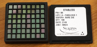
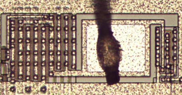
If you were expecting a handy DIP8, you might be disappointed. While some DIY friendly packages would be nice, right now the ASICs ship as wafer level chip scale package (WLCSP) with an unforgiving 0.5 mm pitch. If you can believe it, that’s actually an improvement over the first run, which shipped out as a bare die. Of course as Matt pointed out, anyone who’s gotten to the point of designing their own custom ASIC probably won’t be scared off by the prospect of some fine-pitch soldering. Some in the Chat wondered about the difficulty in getting compatible PCBs produced, but Matt said that in his experience OSH Park has been up to the challenge.

Like the Metal 3D Printing Hack Chat before it, this week’s session went over a topic that’s on the absolute cutting edge of what’s possible for hardware hackers and hobbyists. Truth be told, the vast majority of the people reading Hackaday are no more likely to send away for their own custom ASIC as they are to battle x-rays in an attempt to sinter metal with a homebrew electron gun. But that doesn’t make the fact that some folks out there doing it any less important, or inspiring. That said, if you do end up being one of those select few that can boast they’ve designed a custom chip of their own — don’t forget to send one of them our way.

We’re grateful Matt Venn was able, once again, to share his valuable experience in the realm of open source application-specific integrated circuits with us. If you haven’t checked them out already, the Zero to ASIC workshop he ran for Remoticon 2020 and his talk Open Source ASICs – A Year in Perspective from Remoticon 2021 are required viewing if you want to learn more about this fascinating new frontier in hardware hacking.


The Hack Chat is a weekly online chat session hosted by leading experts from all corners of the hardware hacking universe. It’s a great way for hackers connect in a fun and informal way, but if you can’t make it live, these overview posts as well as the transcripts posted to Hackaday.io make sure you don’t miss out.

Al Williams Tells All In The Logic Simulation Hack Chat

The list of requirements for hosting one of our weekly Hack Chats is pretty short: you’ve got to be knowledgeable, passionate, and above all else, willing to put those two quantities on display for a group of like-minded strangers. Beyond that, we’re not too picky. From industry insider to weekend hobbyist, high school dropout to double doctorate, if you’ve got something interesting to talk about, we’re ready to listen.

But in casting a such a wide net, we occasionally forget that we’ve got a considerable collection of potential hosts within our own worldwide roster of contributors. Among this cast of characters, few can boast the same incredible body of knowledge as Al Williams, who was able to pencil in some time this week to host the Logic Simulation Hack Chat.

Or at least, that was the idea. In reality the Chat covered a wide range of topics, and was peppered with fascinating anecdotes pulled from Al’s decades of experience in the field. Though to be fair, we expected no less. He was building hardware before many of us were born, and can take credit for designs that have been at the bottom of the ocean as well as launched into orbit. He’s been writing about it just as long too, with articles of his appearing in iconic print magazines such as Dr. Dobb’s Journal.

Al has seen and done so much that he still surprises us with the occasional nugget, and we’ve been working with him for years. It was only a week or two back that he started a story with “Back when I used to manage a gas pipeline…” in the middle of a conversation about utility metering.

Of course, that’s not to say some technical discussion didn’t sneak in there from time to time. Sure Al’s  recollection of how they used to literally crawl over the schematics for the 68000 back at Motorola might stick out as a particular high point, but he also explains his personal preference for vendor-specific software tools over their more generic open source counterparts. He also draws comparisons between hardware description languages (HDLs) like Verilog and parametric CAD tools such as OpenSCAD in the way that they help model complex relationships in ways that can’t be easily done by more traditional means.

At one point the conversation lingers on the design and production of application-specific integrated circuits (ASICs), and how they compare to field-programmable gate arrays (FPGAs). Traditionally ASICs have been out of reach for the hobbyist, but with the recent collaboration between Google and SkyWater Technology to create an open source process design kit (PDK), they’re now within the capabilities of a dedicated individual. Matt Venn spoke on the topic during Remoticon 2021, and it’s good to see more folks in the community openly discussing the possibilities of custom silicon designed by hackers.

From there, things start really getting wild. From dreaming of virtual reality circuit simulators that let you fly amongst your creations like in Tron, to salivating over high-end technologies such as reflective memory, this Chat really runs the gamut. But then, that’s sort of why we hold them in the first place. Whether you actively participate or are just along for the ride, the Hack Chat gives everyone in the community a chance to gather around a virtual water cooler with fascinating characters that you won’t find anywhere else.


The Hack Chat is a weekly online chat session hosted by leading experts from all corners of the hardware hacking universe. It’s a great way for hackers connect in a fun and informal way, but if you can’t make it live, these overview posts as well as the transcripts posted to Hackaday.io make sure you don’t miss out.