Pulsed Deposition Points A Different Path To DIY Semiconductors

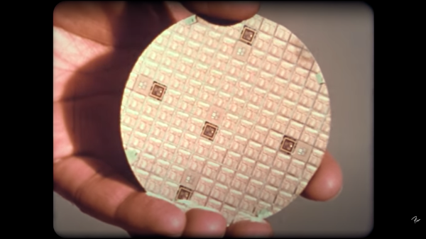
While not impossible, replicating the machines and processes of a modern semiconductor fab is a pretty steep climb for the home gamer. Sure, we’ve seen it done, but nanoscale photolithography is a demanding process that discourages the DIYer at every turn. So if you want to make semiconductors at home, it might be best to change the rules a little and give something like this pulsed laser deposition prototyping apparatus a try.

Rather than building up a semiconductor by depositing layers of material onto a silicon substrate and selectively etching features into them with photolithography, [Sebastián Elgueta]’s chips will be made by adding materials in their final shape, with no etching required. The heart of the process is a multi-material pulsed laser deposition chamber, which uses an Nd:YAG laser to ablate one of six materials held on a rotating turret, creating a plasma that can be deposited onto a silicon substrate. Layers can either be a single material or, with the turret rapidly switched between different targets, a mix of multiple materials. The chamber is also equipped with valves for admitting different gases, such as oxygen when insulating layers of metal oxides need to be deposited. To create features, a pattern etched into a continuous web of aluminum foil by a second laser is used as a mask. When a new mask is needed, a fresh area of the foil is rolled into position over the substrate; this keeps the patterns in perfect alignment.

We’ve noticed regular updates on this project, so it’s under active development. [Sebastián]’s most recent improvements to the setup have involved adding electronics inside the chamber, including a resistive heater to warm the substrate before deposition and a quartz crystal microbalance to measure the amount of material being deposited. We’re eager to see what else he comes up with, especially when those first chips roll off the line. Until then, we’ll just have to look back at some of [Sam Zeloof]’s DIY semiconductors.

Homebrew Electron Beam Lithography With A Scanning Electron Microscope

If you want to build semiconductors at home, it seems like the best place to start might be to find a used scanning electron microscope on eBay. At least that’s how [Peter Bosch] kicked off his electron beam lithography project, and we have to say the results are pretty impressive.

Now, most of the DIY semiconductor efforts we’ve seen start with photolithography, where a pattern is optically projected onto a substrate coated with a photopolymer resist layer so that features can be etched into the surface using various chemical treatments. [Peter]’s method is similar, but with important differences. First, for a resist he chose poly-methyl methacrylate (PMMA), also known as acrylic, dissolved in anisole, an organic substance commonly used in the fragrance industry. The resist solution was spin-coated into a test substrate of aluminized Mylar before going into the chamber of the SEM.

As for the microscope itself, that required a few special modifications of its own. Rather than rastering the beam across his sample and using a pattern mask, [Peter] wanted to draw the pattern onto the resist-covered substrate directly. This required an external deflection modification to the SEM, which we’d love to hear more about. Also, the SEM didn’t support beam blanking, meaning the electron beam would be turned on even while moving across areas that weren’t to be exposed. To get around this, [Peter] slowed down the beam’s movements while exposing areas in the pattern, and sped it up while transitioning to the next feature. It’s a pretty clever hack, and after development and etching with a cocktail of acids, the results were pretty spectacular. Check it out in the video below.

It’s pretty clear that this is all preliminary work, and that there’s much more to come before [Peter] starts etching silicon. He says he’s currently working on a thermal evaporator to deposit thin films, which we’re keen to see. We’ve seen a few sputtering rigs for thin film deposition before, but there are chemical ways to do it, too.

Continue reading “Homebrew Electron Beam Lithography With A Scanning Electron Microscope”

Unusual Tool Gets An Unusual Repair

In today’s value-engineered world, getting a decade of service out of a cordless tool is pretty impressive. By that point you’ve probably gotten your original investment back, and if the tool gives up the ghost, well, that’s what the e-waste bin is for. Not everyone likes to give up so easily, though, which results in clever repairs like the one that brought this cordless driver back to life.

The Black & Decker “Gyrodriver,” an interesting tool that is controlled with a twist of the wrist rather than the push of a button, worked well for [Petteri Aimonen] right up until the main planetary gear train started slipping thanks to stripped teeth on the plastic ring gear. Careful measurements of one of the planetary gears to determine parameters like the pitch and pressure angle of the teeth, along with the tooth count on both the planet gear and the stripped ring.

Here, most of us would have just 3D printed a replacement ring gear, but [Petteri] went a different way. He mentally rolled the ring gear out, envisioning it as a rack gear. To fabricate it, he simply ran a 60° V-bit across a sheet of steel plate, creating 56 parallel grooves with the correct pitch. Wrapping the grooved sheet around a round form created the ring gear while simultaneously closing the angle between teeth enough to match the measured 55° tooth angle in the original. [Petteri] says he soldered the two ends together to form the ring; it looks more like a weld in the photos, but whatever it was, the driver worked well after the old plastic teeth were milled out and the new ring gear was glued in place.

We think this is a really clever way to make gears, which seems like it would work well for both internal and external teeth. There are other ways to do it, of course, but this is one tip we’ll file away for a rainy day.

Integrated Circuit Manufacturing At Bell Labs In 1983

With the never ending march of technological progress, arguably the most complex technologies become so close to magic as to be impenetrable to those outside the industry in which they operate. We’ve seen walkthrough video snapshots of just a small part of the operation of modern semiconductor fabs, but let’s face it, everything you see is pretty guarded, hidden away inside large sealed boxes for environmental control reasons, among others, and it’s hard to really see what’s going on inside.

Let’s step back in time a few decades to 1983, with an interesting tour of the IC manufacturing facility at Bell Labs at Murray Hill (video, embedded below) and you can get a bit more of an idea of how the process works, albeit at a time when chips hosted mere tens of thousands of active devices, compared with the countless billions of today. This fab operates on three inch wafers, producing about 100 die each, with every one handled and processed by hand whereas modern wafers are much bigger, die often much smaller with the total die per wafer in the thousands and are never handled by a filthy human.

Particle counts of 100 per cubic foot might seem laughable by modern standards, but device geometries back then were comparatively large and the defect rate due to it was not so serious. We did chuckle somewhat seeing the operator staff all climb into their protective over suits, but open-faced with beards-a-plenty poking out into the breeze. Quite simply, full-on bunny suits were simply not necessary. Anyway, whilst the over suits were mostly for the environment, we did spot the occasional shot of an operator wearing some proper protective face shielding when performing some of the higher risk tasks, such as wafer cleaning, after all as the narrator says “these acids are strong enough to eat through the skin” and that would certainly ruin your afternoon.

No story about integrated circuit processing would be complete without mentioning the progress of [Sam Zeloof] and his DIY approach to making chips, and whilst he’s only managing device counts in the hundreds, this can only improve given time.

Continue reading “Integrated Circuit Manufacturing At Bell Labs In 1983”

Scratch-Built Electric Buggy Tears Up The Dunes

It’s a fair bet to say that the future of personal transportation will probably be electric. In support of that, every major car manufacturer either has an electric drivetrain option available now, or they’re working furiously on developing one. And while it’s good that your suburban grocery grabber will someday be powered by the sun, what about the pressing need for EVs that are just plain fun to drive?

To fill the fun gap, at least for now, [James Biggar] built what you can’t buy: an all-electric dune buggy. And lest you think this was a kit build, be assured that the summary video below shows this little sand rail was 100% scratch-built. The chassis is fabricated from bent tubing, and welded up using a clever plywood template to get the angles just right. The buggy has four-wheel independent suspension and a wide, aggressive stance to handle rough terrain. The body panels are sheet aluminum bent on a custom-built brake, which was also used to form the Plexiglas windshield with a little help from a heat gun.

While the bodywork makes the buggy pretty sick looking, the drivetrain is just as impressive. [James] used an ME1616, a liquid-cooled 55-kW beast. A chain drive couples the motor to a differential from a Honda CR-V which has a limited-slip modification installed. The batteries are impressive, too — 32 custom-made lithium-iron-phosphate batteries made from 32650 cells in vacuum-formed ABS plastic shells that nest together compactly. It all adds up to a lot of fun in the dirt; skip to 23:37 in the video to see what this thing can do.

Honestly, the level of craftsmanship here is top-notch, and is all the more impressive in that it’s not fancy — just good, solid methods and lots of hard work. We’d love to have the time and resources to put into something like this — although a drop-in crate motor EV might be a satisfying build too.

Continue reading “Scratch-Built Electric Buggy Tears Up The Dunes”

Custom-Fit Small Shop Crane Lightens The Load

On the shortlist of workshop luxuries, we’d bet a lot of hackers would include an overhead crane. Having the ability to lift heavy loads safely and easily opens up a world of new projects, and puts the shop into an entirely different class of capabilities.

As with many of us, [Jornt] works in a shop with significant space constraints, so the jib crane he built had to be a custom job. Fabricated completely from steel tube, the build started with fabricating a mast to support the crane and squeezing it into a small slot in some existing shelves in the shop, which somehow didn’t catch on fire despite being welded in situ. A lot of custom parts went into the slewing gear that mounts the jib, itself a stick-built space frame that had to accommodate a pitched ceiling. A double row of tubing along the bottom of the jib allows a trolley carrying a 500 kg electric winch to run along it, providing a work envelope that looks like it covers the majority of the shop. And hats off for the safety yellow and black paint job — very industrial.

From the look of the tests in the video below, the crane is more than up to the task of lifting engines and other heavy loads in the shop. That should prove handy if [Jornt] tackles another build like his no-compromises DIY lathe again.

Continue reading “Custom-Fit Small Shop Crane Lightens The Load”

Bike On Over To The Campground

Like many of us, [Paul] enjoys occasionally hitching up his tow-behind camper and heading out to the wilderness to get away from it all at his favorite campsite. Unlike the vast majority of those who share his passion for the outdoors, though, [Paul] is hitching his camper up to a bicycle. Both the camper and the bike are custom built from the ground up, and this video shows us a little more details on [Paul]’s preferred mode of transportation.

While he is known for building custom vehicles of one sort or another, this latest one is a more traditional bicycle frame that he has modified only slightly to fit a recumbent-style seat and a small gas-powered motor. Even though the motor is decades old, it started right up and gives the power needed to pull the custom camper. [Paul] builds one-person campers like this out of corrugated plastic for durability and light weight, and this one is specifically designed for his size and sleeping style. It includes everything needed for a night under the stars, too, including a stove, storage compartments, and a few windows.

With the bike and camper combined weighing in at just over 200 pounds, the motor can be used as a pedal-assist device thanks to the clever engineering behind a front-wheel-drive pedal system on this bike. With all of that custom fabrication, [Paul] is free to head out to the wilderness without all the encumbrances (and high price) of traditional motor vehicle-based camping. For those curious about some of [Paul]’s other vehicle creations, take a look at this tiny speedboat for one.

Continue reading “Bike On Over To The Campground”