Clearly The Best Way To Organize SMD Parts

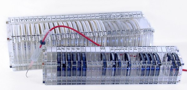
Have some plexiglas (acrylic) leftovers lying around? Well, they could be put to good use in making this SMD organizer. It comes in handy if you deal with a lot of SMD components in your work. No longer will you waste your time trying to find a 15K 1206 resistor, or that BAS85 diode… or any other component you can think of soldering on the PCB. The basic idea is fairly straightforword, which helped keep this short.

2SMD resistors are packed in thick paper tapes that don’t bend easily, and thus need larger containers than other components, which are packed mainly in flexible PE tapes. The first version of this organizer was built with a 96mm diameter space for resistors and 63mm diameter for other components, but it seems that there is no need for such large compartments. If I were to make it again, I would probably scale everything down to about 80% of it’s current size.

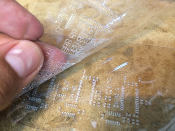
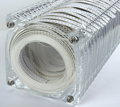
The best way to join all plexiglass parts is to use four M4 threaded rods. There is also a 1.5mm steel rod which holds SMD tape ends in place and helps to un-stick the transparent tape which covers the components. At the top of the organizer there is a notch for paper, used for components labels. Most SMD components are packed in 8mm wide tapes, making the optimal compartment width 10mm. It is not easy to cut the 10mm thick acrylic and get a neat edge – instead, you could use more layers of thin sheets to make the spacers. Using 5mm acrylic you can combine more layers for any width of tape, which contains wider components, like SMD integrated circuits. The only thing that you have to be careful about, is to keep the distance between the thin steel rod and acrylic, which is marked as “2-4mm” on the drawing. It is good if this space is just a few tenths of a millimeter wider than the thickness of SMD tapes.

smd_ortho
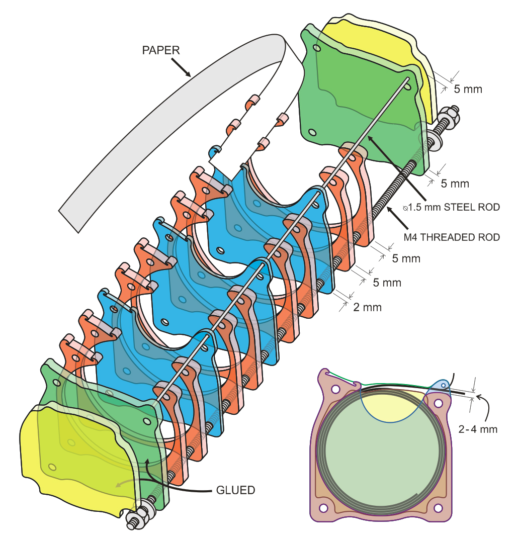
The CorelDraw file that can be used for laser cutting the acrylic parts, is available for download. If you scale the profiles, don’t forget to readjust the hole diameters and some other dimensions which have to remain intact. If you have 5mm acrylic pieces, you should probably use two layers of acrylic for every tape (red parts on the drawing). The barrier layers would be made of thin acrylic — for instance 2mm (the blue parts). Edge layers (green) are once again 5mm thick, and there are also the end pieces (yellow), glued to the previous borders and used to “round up” the whole construction and to protect your hands from the threaded rods and nuts.

While you’re building this for your bench, make a vacuum picking tool for SMDs out of a dispensing syringe with a thick needle. It’s a common trick for hackers to use an aquarium air pump, just turn the compressor unit by 180°, so that it creates vacuum instead of blowing the air outside. This process is described by R&TPreppers in the video below.

Continue reading “Clearly The Best Way To Organize SMD Parts”

Surface Mount Soldering Workshop Shares Secrets Of CM

Friday afternoon I had the pleasure of sitting in on a surface mount soldering workshop. I’ve done some surface mount soldering before and am quite adept with a soldering iron, but this focused on solder paste and a hot air pencil. [Bob Cogeshall] ran the workshop and went beyond the most basic information. His experience founding Small Batch Assembly, a contract manufacturer whose offices are in the Nova Labs hackerspace, has led him to learn a lot of tricks of the trade.

Continue reading “Surface Mount Soldering Workshop Shares Secrets Of CM”

Understanding Surface Mount

Do you know what a MELF is (and, yes, it is safe for work to Google it)? What’s the difference between a QFP, and LCC, and a PLCC package? Do you need a 0603 resistor or a 1206 resistor?

If you are an old hand at surface mount devices (SMDs) you probably know the answers to most of these questions. But if you’ve done most of your work with through hole, it is a confusing mess of acronyms and numbers. Sure, you can Google and find out that at 0603 resistor is .06 inches by .03 inches. [TopLine] has a great booklet that pulls many common definitions in one place available for download that can help you make sense of different SMD nomenclature.

Continue reading “Understanding Surface Mount”

Swapping Dev Board Crystals To Suit Your Needs

Microcontroller Dev Boards have the main hardware choices already made for you so you can jump right into the prototyping by adding peripherals and writing code. Some of the time they have everything you need, other times you can find your own workarounds, but did you ever try just swapping out components to suit? [Andy Brown] documented his process of transplanting the clock crystal on an STM32F4 Discovery board.

Even if you don’t need to do this for yourself, the rework process he documented in the clip after the break is fun to watch. He starts by cleaning the through-hole joints of the crystal oscillator with isopropyl alcohol and then applies some flux paste to each. From there the rest is all hot air. The crystal nearly falls out due to gravity but at the end he needs to pluck it out with his fingers. We’re happy to see others using this “method” as we always feel like it’s a kludge when we do it. Next he grabs the load caps with a pair of tweezers after the briefest of time under the heat.

We’d like to have a little bit of insight on the parts he replaces and we’re hoping there are a few crystal oscillator experts who can leave a comment below. [Andy] calculates a pair of 30pf load caps for this crystal. We understand the math but he mentions a common value for board and uC input capacitance:

assuming the commonly quoted CP + CI = 6pF

So we asked and [Andy] was kind enough to share his background on the topic:

It’s a general “rule of thumb” for FR4 that the stray capacitance due to the traces on the board and the input (lead) capacitance of the the MCU is in in the range of 4-8pF. I’m used to quoting the two separately (CP,CI) but if you look around you’ll see that most people will combine the two and call it just “CP” and quote a value somewhere between 4 and 8pF. It’s all very “finger in the air” and for general purpose MCU clocks you can get away picking the mid-value and be done with it.

That leaves just one other question; the original discovery board had an in-line resistor on one of the crystal traces which he replaces with a zero ohm jumper. Is it common to include a resistor and what is the purpose for it?

Continue reading “Swapping Dev Board Crystals To Suit Your Needs”

A DIY Pick And Place You Can Build Right Now

There have been quite a few DIY pick and place projects popping up recently, but most of them are limited to conceptual designs or just partially working prototypes. [Juha] wrote in to let us know about his project, LitePlacer, which is a fully functional DIY pick and place machine with working vision that can actually import BOMs and place parts as small as 0402 with pretty good accuracy.

LitePlacer UI
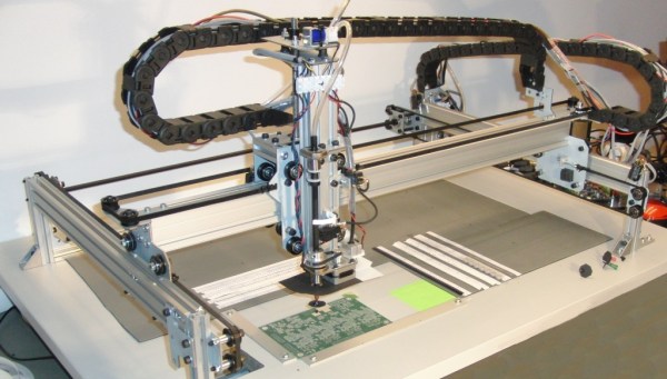
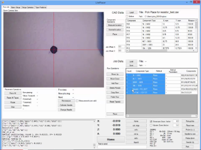
While some other DIY pick and place setups we’ve featured use fairly exotic setups like delta bots, this machine is built around typical grooved bearings and extruded aluminum. The end effector includes a rotating vacuum tip and a camera mounted alongside the tip. The camera provides feedback for locating fiducials and for finding the position of parts. Instead of using feeders for his machine, [Juha] opted to pick parts directly from pieces of cut tape. While this might be inconvenient if you’re placing large quantities of a single part, it helps keep the design simple.

The software that runs the machine is pretty sophisticated. After a bit of configuration it’s able to import a BOM with X/Y information and start placing within seconds. It also uses the camera to calibrate the needle, measure the PCB  using the fiducials, and pinpoint the location of cut tape sections.

If you want to build your own machine, [Juha] published detailed instructions that walk you through the entire assembly process. He’s also selling a kit of parts if you don’t want to source everything yourself. Check out the video after the break to see the machine import a BOM and place some parts (all the way down to 0402).

Continue reading “A DIY Pick And Place You Can Build Right Now”

Add A Bluetooth Interface To Your Kitchen Scale

Kitchen scale

When [Adam] found himself in need of a force meter, he didn’t want to shell out the cash for a high-end model. Instead, he realized he should be able to modify a simple and inexpensive kitchen scale to achieve the results he desired.

The kitchen scale [Adam] owned was using all through hole components on a double-sided PCB. He was able to easily identify all of the IC’s and find their datasheets online. After doing some research and probing around with a frequency counter, he realized that one of the IC’s was outputting a frequency who’s pulse width was directly proportional to the amount of weight placed on the scale. He knew he should be able to tap into that signal for his own purposes.

[Adam] created his own custom surface mount PCB, and used an ATMega8 to detect the change in pulse width. He then hooked up a Bluetooth module to transmit the data wirelessly. These components required no more than 5V, but the scale runs from two 3V batteries. Using what he had on hand, [Adam] was able to lower the voltage with just a couple of diodes.

[Adam] managed to cram everything into the original case with little modification. He is now considering writing an Android application to interface with his upgraded kitchen scale.

Solder Stencil

How To Laser Cut Mylar Solder Stencils

When you think about the difficulties of working with surface mount components, the first thing that often comes to mind is trying to solder those tiny little parts. Instead of soldering those parts by hand, you can actually apply solder paste to the pads and place all of the components on at once. You can then heat up the entire board so all of the parts are soldered simultaneously. It sounds so much easier! The only problem is you then need a solder stencil. You somehow have to get a thin sheet of material that has a perfectly sized hole where all of your solder pads are. It’s not exactly trivial to cut them out by hand.

[Juan] recently learned a new trick to make cutting solder stencils a less painful process. He uses a laser cutter to cut Mylar sheets into stencils. [Juan] appears to be using EagleCAD and Express PCB. Both tools are available for free to hobbyists. The first step in the process is to export the top and bottom cream layers from your CAD software.

The next step is to shrink the size of the solder pads just a little bit. This is to compensate for the inevitable melting that will be caused by the heat from the laser. Without this step, the pads will likely end up a little bit too big. If your CAD software exports the files as gerbers, [Juan] explains how to re-size the pads using ViewMate. If they are exported as DXF files, he explains how to scale them using AutoCAD. The re-sized file is then exported as a PDF.

[Juan’s] trick is to actually cut two pieces of 7mil Mylar at the same time. The laser must be calibrated to cut all the way through the top sheet, but only part way into the bottom piece. The laser ends up slightly melting the edges of the little cut out squares. These then get stuck to the bottom Mylar sheet. When you are all done cutting, you can simply pull the sheets apart and end up with one perfect solder stencil and one scrap piece. [Juan] used a Full Spectrum 120W laser cutter at Dallas Makerspace. If you happen to have this same machine, he actually included all of the laser settings on his site.