One of the joys of an itinerant existence comes in periodically being reunited with the fruits of various orders that were sent to hackerspaces or friends somewhere along the way. These anonymous parcels from afar hold an assortment of wonders, with the added element of anticipation that comes from forgetting exactly what had been ordered.
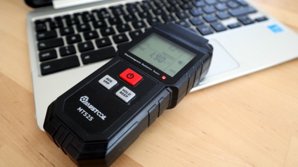
So it is with today’s subject, a Mustool MT525 electromagnetic radiation tester. At a cost not far above £10 ($13.70), this was an impulse purchase driven by curiosity; these devices claim to measure both magnetic and electric fields, but what do they really measure? My interest in these matters lies in the direction of radio, but I have never examined such an instrument. Time to subject it to the Hackaday treatment.
When [Kenneth Keiter] took apart his Starlink dish back in November, he did his best to explain the high-level functionality of the incredibly complex device in a video posted to his YouTube channel. It was a fascinating look at the equipment, but by his own admission, he wasn’t the right person to try and explain the nuances of how the phased array actually functioned. But he knew who could do the technology justice, which is why he shipped the dismembered dish over to [Shahriar Shahramian] of The Signal Path.
Don’t be surprised if you can’t quite wrap your head around his detailed analysis after your first viewing. You’ll probably have a few lingering questions after the second re-watch as well. But that’s OK, as [Shahriar] still has a few of his own. Even after cutting out a section of the dish and putting it under an X-ray, it’s still not completely clear how the SpaceX engineers managed to cram everything into such a tidy package. Though there seems to be no question that the $500 price for the early-access hardware is an absolute steal, all things considered.
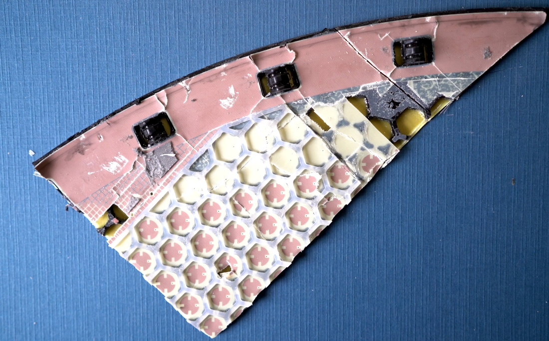
The layered antenna works on multiple frequencies.
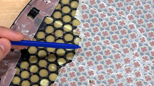
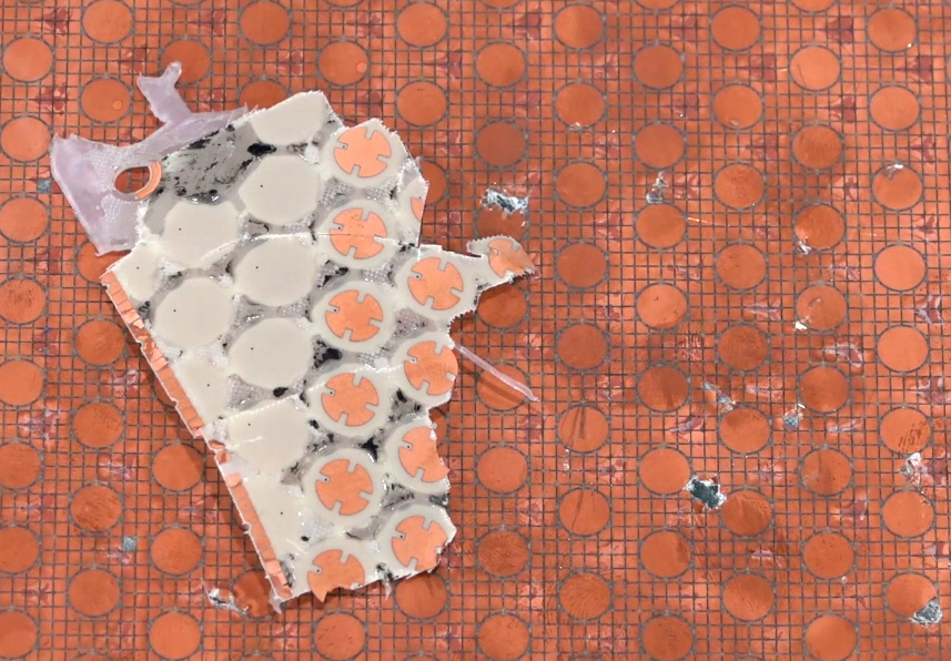
Most of the video is spent examining the stacked honeycomb construction of the phased antenna array, which as expected, holds a number of RF secrets if you know what to look for. Put simply, there’s no such thing as an insignificant detail to the trained eye. From the carefully sized injection molded spacer sheet that keeps the upper array a specific distance from the RF4-like radome, to the almost microscopic holes that have been bored through each floating patch to maintain equalized air pressure through the stack up, [Shahriar] picks up on fascinating details which might otherwise seem like arbitrary design decisions.
But a visual inspection will only get you so far. Eventually [Shahriar] has to cut out a slice of the PCB so he can fit it into the X-ray machine, but don’t feel too bad, the dish was long dead before he got his hands on it. While he hasn’t yet completed his full analysis, an initial examination indicates that each large IC and the eight chips surrounding it make up a 16 channel beam forming module. Each channel is further split into two RX and TX pairs, which provides the necessary right and left hand polarization. That said, he admits there’s some room for interpretation and that further work would be necessary before any hard conclusions could be made.
Between this RF analysis and the initial overview provided by [Kenneth], we’ve already learned a lot more about this device than many might have expected considering how rare and expensive the hardware is. While we admit it’s not immediately clear what kind of hijinks hardware hackers could get into once this device is fully understood, we’re certainly eager to find out.
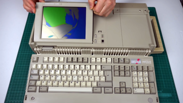
If someone gifted you a cheap laptop this holiday season, you might be a little put out by the 2GB of RAM and the 400 MHz CPU. However, you might appreciate it more once you look at [Noel’s Retro Lab’s] 4.8 Kg Amstrad PPC512 He shows it off inside and out in the video below.
Unlike a modern laptop, this oldie but goodie has a full keyboard that swings out of the main body. The space below the keyboard contains the LCD screen, which [Noel] is going to have to replace with an LCD from another unit that was in worse shape but had a good-looking screen. In this video, he gets as far as getting video output to an external monitor, but neither LCD shows any sign of life. But he’s planning more videos soon.
We’re always pleased to see one of our community’s projects succeed, and we celebrate that success in whatever what it comes. But seeing a company launched to commercialize an idea that started as a Hackaday.io project and a Hackaday Prize entry is especially gratifying. So we were pleased as punch to see that MAKESafe Tools has managed to bring the idea of add-on machine tool braking to market. We’d love to add this to several tools in our shop. Honestly, of all the terrifying ways machine tools can slice, dice, and shred human flesh asunder, we always considered the lowly bench grinder fairly low-risk — and then we had a chance to “Shake Hands with Danger.”
Another great thing about the Hackaday community is the way we all try to keep each other up to speed on changes and news that affects even our smallest niches. Just last week Tom Nardi covered a project using the venerable TI eZ430-Chronos smartwatch as a makeshift medical alert bracelet for a family member. It’s a great application for the proto-smartwatch, but one eagle-eyed commenter helpfully pointed out that TI is shutting down their processors wiki in just a couple of weeks. The banner at the top of each page warns that the wiki is not read-only and that any files needed should be downloaded by January 15. Also helpfully, subsequent comments include instructions to download the entire wiki and a torrent link to the archive. It’s always sad to see a platform lose support, especially one that has gained a nice following, but it’s heartening to see the community pull together to continue to support each other like this.
We came across an interesting article this week that’s was a fascinating glimpse into how economic forces shape and drive technological process, and vice versa. It turns out that some of the hottest real estate commodities these days are the plots of land occupied by AM radio stations serving metropolitan markets. It’s no secret that terrestrial radio in general, and AM radio in particular, are growing increasingly moribund, and the infrastructure needed to keep them on the air is getting harder and harder to justify. Chief among these are the large tracts of land devoted to antenna farms, which are often located in suburban and exurban areas near major cities. They’re tempting targets for developers looking to plunk down the physical infrastructure needed to support “New Economy” players like Amazon, which continue to build vast automated warehouses in areas that are handy to large customer bases. It’s a bit sad to watch a once mighty industry unravel and be sold off like this, but such is the nature of progress.
And finally, you may recall a Links article mention a few weeks back about a teardown of a super-sized IBM processor module. A quarter-million dollar relic of the 1990s, the huge System/390 module was an engineering masterpiece that met an unfortunate end at the hands of EEVblog’s Dave Jones. As a follow-up, Dave teamed up with fellow YouTuber CPU Galaxy to take a less-destructive tour of the module using X-ray analysis. The level of engineering needed for a 64-layer ceramic backplane is astonishing, and Dave’s play-by-play is pretty entertaining too. As a bonus, CPU Galaxy has some really interesting stuff; his place is basically a museum of vintage tech, and he just earned a new sub.
“I don’t get mad when people rip me off. I actually think its kinda cool, because imitation is the sincerest form of flattery.” — Ben Heckendorn
For some “hacking things together” can mean heavily borrowing from other’s work in order to make a new, derivative work. Though longtime hardware hacker, Ben Heckendorn, didn’t expect one of his early SNES handheld projects to become the inspiration for a Famicom-style clone console. There have been a number of clone consoles available online for years, and all have been made to varying levels of build quality. The subject clone console in question is called the Easegmer 12-bit Retro Console, so [Ben] decided to record his teardown of the handheld borrowing from his original design. (Video, embedded below.)
The Easegmer handheld has a “surprising” list of features according to its packaging including: sports games, logic games, memoyr games, USB charger management, double power supply option, and dirunal double backlight option. All big (and slightly misspelled) promises though the most egregious claim has to be that, “No violent games, your child’s body and mind get full exercise.”. The statement may have a modicum of truth to it, except for the fact that game 84 of 220 is literally named “Violent”. Dunking aside, the handheld does feature a standard size rechargeable battery in addition to the option of powering the device with three AAA batteries. There’s even a “fun size” screwdriver and a few replacement screws included which is more than you can say for most modern electronics.
It has been almost twenty years after [Ben] originally published his SNES portable project on his website. So as a long awaited follow-up, [Ben] plans to make a “meta-portable”. This meta portable will start with the Adobe Illustrator files he kept from that SNES portable in 2001 and incorporate pieces of the Easegmer clone console. Thus spawning a new clone of the clone of his clone…or whatever that project ends up being its sure to be worth repeating.
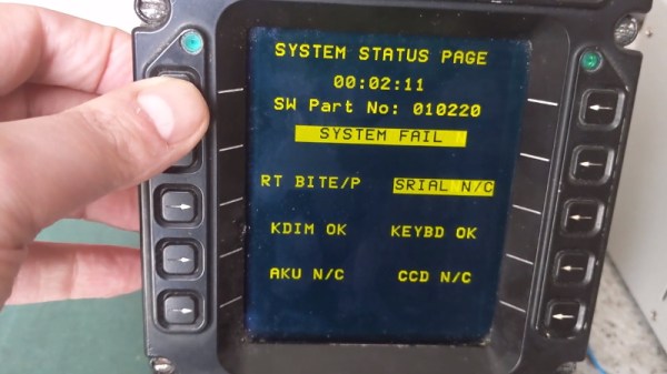
The second hand market is a wonderful thing; you never know what you might find selling for pennies on the dollar simply because it’s a few years behind the curve. You might even be able to scrounge up some electronics pulled out of a military aircraft during its last refit. That seems to be how [Adrian Smith] got his hands on a Control Display Unit (CDU) originally installed in a Royal Air Force AgustaWestland AW101 “Merlin” helicopter. Not content to just toss it up on a shelf, he decided to take a look inside of the heavy-duty cockpit module and see if he couldn’t make some sense out of how it works.
Unsurprisingly, [Adrian] wasn’t able to find much information on this device on the public Internet. The military are kind of funny like that. But a close look at the burn-in on the CDU’s orange-on-black plasma display seems to indicate it had something to do with the helicopter’s communication systems. Interestingly, even if the device isn’t strictly functional when outside of the aircraft, it does have a pretty comprehensive self-test and diagnostic system on-board. As you can see in the video after the break, there were several menus and test functions he was able to mess around with once it was powered up on the bench.
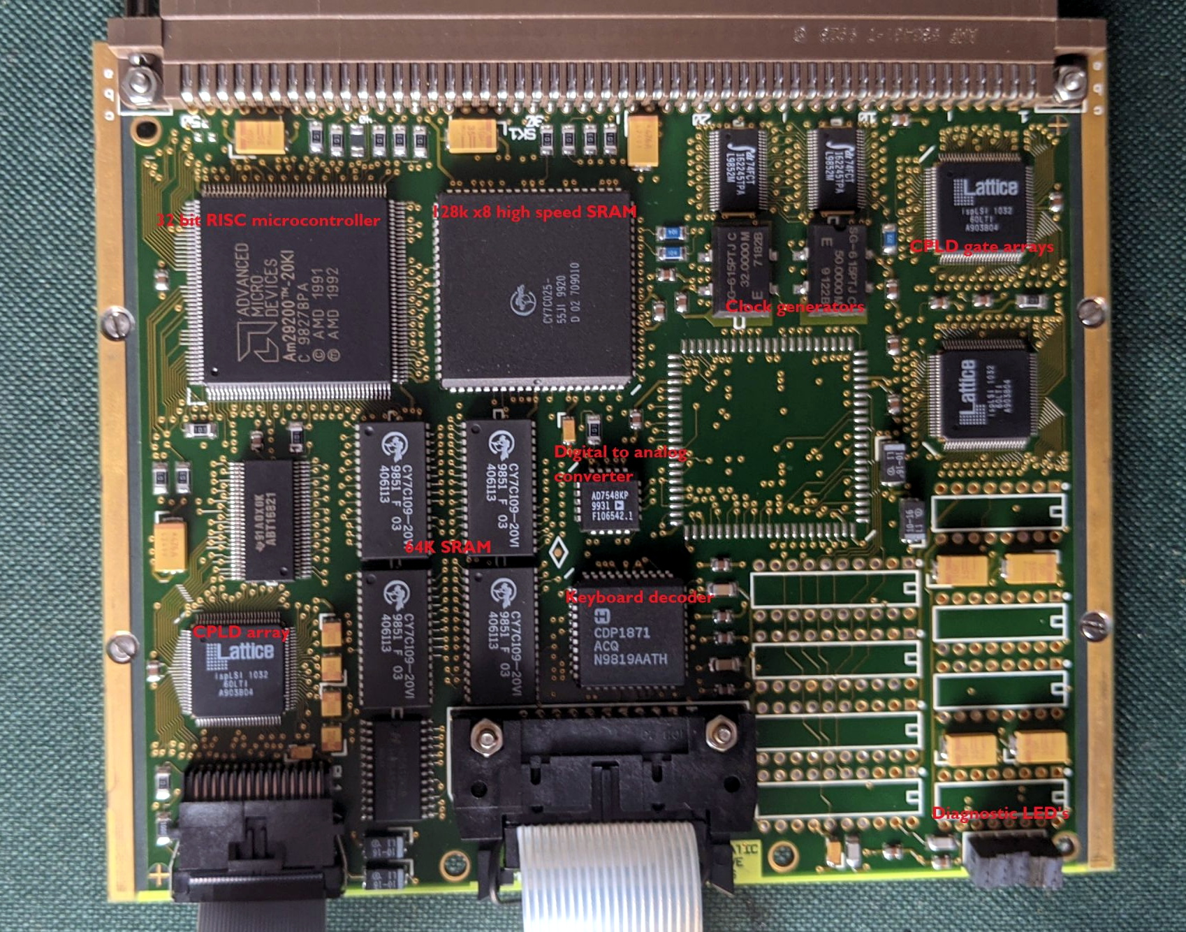
With the case cracked open, [Adrian] found three separate PCBs in addition to the display and keyboard panel on the face of the CDU. The first board is likely responsible for communicating with the helicopter’s internal systems, as it features a MIL-STD-1553B interface module, UART chips, and several RS-232/RS-485 transceivers. The second PCB has a 32-bit AMD microcontroller and appears to serve as the keyboard and display controller, possibly also providing the on-board user interface. The last board looks to be the brains of the operation, with a 25 MHz Motorola 68EC020 CPU and 1Mb of flash.
All of the hardware inside the CDU is pretty generic, but that’s probably the point. [Adrian] theorizes that the device serves as something of a generic pilot interface module, and when installed in the Merlin, could take on various functions based on whatever software was loaded onto it. He’s found pictures online that seem to show as many as three identical CDUs in the cockpit, all presumably running a different system.
While SpaceX’s constellation of Starlink satellites is nowhere near its projected final size, the company has enough of the birds zipping around in low Earth orbit to start a limited testing period they call the Better Than Nothing Beta. If you’re lucky enough to get selected, you have to cough up $500 for the hardware and another $100 a month for the service. Despite the fairly high bar for getting your hands on one, [Kenneth Keiter] decided to sacrifice his Starlink dish to the teardown Gods.
We say sacrifice because [Kenneth] had to literally destroy the dish to get a look inside. It doesn’t appear that you can realistically get into the exceptionally thin antenna array without pulling it all apart, thanks in part to preposterous amount of adhesive that holds the structural back plate onto the PCB. The sky-facing side of the phased array, the key element that allows the antenna to track the rapidly moving Starlink satellites as they pass overhead, is also laminated to a stack-up comprised of plastic hexagonal mesh layers, passive antenna elements, and the outer fiberglass skin. In short, there are definitely no user-serviceable parts inside.
The dish hides many secrets under its skin.
Beyond attempting to analyze the RF magic that’s happening inside the antenna, [Kenneth] also takes viewers through a tour of some of the more recognizable components of the PCB; picking out things like the Power over Ethernet magnetics, a GPS receiver, some flash storage, and the H-Bridge drivers used to control the pan and tilt motors in the base of the dish.
It also appears that the antenna is a self-contained computer of sorts, complete with ARM processor and RAM to run the software that aims the phased array. Speaking of which, it should come as no surprise to find that not only are the ICs that drive the dizzying array of antenna elements the most numerous components on the PCB, but that they appear to be some kind of custom silicon designed specifically for SpaceX.