Should you ever pick up [Steve Wozniak]’s autobiography, you will learn that in the early 1970s when his friend [Steve Jobs] was working for Atari, [Woz] was designing calculators for Hewlett Packard. It seems scarcely believable today, but he describes his excitement at the prospects for the calculator business, admitting that he almost missed out on the emerging microcomputer scene that would make him famous. Calculators in the very early 1970s were genuinely exciting, and were expensive and desirable consumer items.
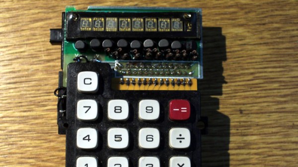
[Amen] has a calculator from that period, a Prinztronic Micro, and he’s subjected it to an interesting teardown. Inside he finds an unusual modular design, with keyboard, processor, and display all having their own PCBs. Construction is typical of the period, with all through hole components, and PCBs that look hand laid rather than made using a CAD package. The chipset is a Toshiba one, with three devices covering logic, display driver and clock.
The Prinztronic is an interesting device in itself, being a rebadged 1972 Sharp model under a house brand name for the British retailer Dixons, and that Toshiba chipset is special because it is the first CMOS design to market. It was one of many very similar basic calculators on the market at the time, but at the equivalent of over 100 dollars in today’s money it would still have been a significant purchase.
Long-tern Hackaday readers will remember we’ve shown you at least one classic calculator rebuild in the past, the venerable 1975 Sinclair!