Pano Logic FGPA Hacking Just Got Easier

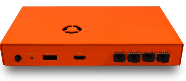
When Pano Logic went out of business in 2012, their line of unique FPGA-based thin clients suddenly became a burden that IT departments didn’t want anything to do with. New and used units flooded the second-hand market, and for a while you could pick these interesting gadgets up for not much more than the cost of shipping. Thanks to considerable interest from the hacking community the prices for these boxes have climbed a bit on eBay, but they’re still a great way to get your feet wet with FPGA hacking.

Especially now, as Pano Logic fanatic [Skip Hansen] has figured out how to flash a new firmware on them without having to crack open the case and break out the JTAG or SPI programmer. For the seasoned hardware hacker that might not seem like a big deal, but if you’re new to the game or just more interested in the software side of the equation, this trick makes things considerably more accessible. Having an external programmer is still a good idea if things go south, but if you’re just looking to flash some demos and see what the hardware is capable of this is a huge quality of life improvement.

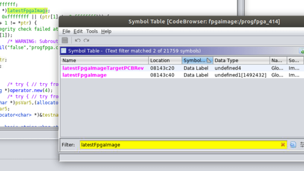
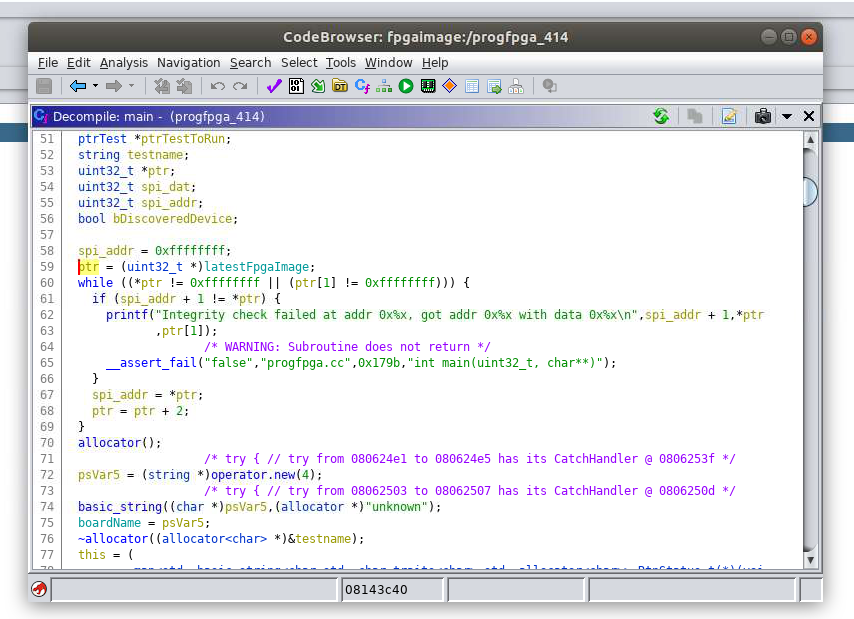
Even if you aren’t interested in fiddling with the orphaned products of a defunct Bay Area startup, the write-up is a fascinating look at practical software reverse engineering. As it turns out, [Skip] didn’t create this new firmware update tool from scratch. He actually opened up the official Linux update utility from Pano Logic in Ghidra and was able to figure out where the firmware image actually lived inside the program. He then wrote his own tool in C which will patch the update tool with a user-supplied firmware image.

After patching, all you need to do is follow the official update procedure, which Pano Logic helpfully documented in the YouTube video after the break. [Skip] mentions he didn’t find any clear license information in the official software he was fiddling with, and of course with the company out of business it’s not too likely anyone is going to come knocking down his door anyway. Still, he says the downloads for the Pano Logic updater are still floating around on the tubes out there for you to find, so he’s not distributing anyone’s code but his own in this project.

There are a number of hackers out there working to turn the Pano Logic thin clients into useful general purpose FPGA platforms, such as [Tom Verbeure], who’s incredible graphics demos got [Skip] inspired to grab his own unit off eBay. With support for USB and SDRAM added by [Wenting Zhang] while getting his FPGA GBA emulator running on the hardware, it seems there’s never been a better time to get on the Pano Logic train.

Continue reading “Pano Logic FGPA Hacking Just Got Easier”

Exostiv FPGA Debugging Might Be A Bargain

Got $4,000 to spend? Even if you don’t, keep reading — especially if you develop with FPGAs. Exostiv’s FPGA debugging setup costs around $4K although if you are in need of debugging a complex FPGA design and your time has any value, that might not be very expensive. Then again, most of us have a lot of trouble justifying a $4,000 piece of test gear. But we wanted to think about what Exostiv is doing and why we don’t see more of it. Traditionally, debugging FPGAs meant using JTAG and possibly some custom blocks that act like a logic analyzer and chew up real estate on your device. Exostiv also uses some of your device, but instead of building a JTAG-communicating logic analyzer it… well, here’s what their website says:

EXOSTIV IP uses the MGTs (Multi-Gigabit Transceivers) to flow captured data out of the FPGA to an external memory. EXOSTIV IP supports repeating captures of up to 32,768 internal nodes simultaneously at the FPGA’s speed of operation (16 data sets x 2,048 bits).

EXOSTIV IP provides dynamic multiplexer controls to capture even more data sets without the need to recompile. Dynamic ON/OFF controls of data sets let you select the data set and preserve the MGT’s bandwidth for when deeper captures of a reduced set of data is required.

In a nutshell, this means they use high-speed communications to send raw data to a box that has memory and connects back to a PC. That means they can store more data, have more data come out of the chip over a certain time frame, and do sophisticated processing. You can see a video about the device below, and there are more detailed videos on their channel, as well.

Continue reading “Exostiv FPGA Debugging Might Be A Bargain”

Is Intel’s Management Engine Broken Yet?

Our own [Brian Benchoff] asked this same question just six months ago in a similar headline. At that time, the answer was no. Or kind of no. Some exploits existed but with some preconditions that limited the impact of the bugs found in Intel Management Engine (IME). But 2017 is an unforgiving year for the blue teams, as lot of serious bugs have been found throughout the year in virtually every fields of computing. Researchers from Positive Technologies report that they found a flaw that allows them to execute unsigned code on computers running the IME. The cherry on top of the cake is that they are able to do it via a USB port acting as a JTAG port. Does this mean the zombie apocalypse is coming?

Before the Skylake CPU line, released in 2015, the JTAG interface was only accessible by connecting a special device to the ITP-XDP port found on the motherboard, inside a computer’s chassis. Starting with the Skylake CPU, Intel replaced the ITP-XDP interface and allowed developers and engineers to access the debugging utility via common USB 3.0 ports, accessible from the device’s exterior, through a new a new technology called Direct Connect Interface (DCI). Basically the DCI provides access to CPU/PCH JTAG via USB 3.0. So the researchers manage to debug the IME processor itself via USB DCI, which is pretty awesome, but USB DCI is turned off by default, like one of the researchers states, which is pretty good news for the ordinary user. So don’t worry too much just yet.

Continue reading “Is Intel’s Management Engine Broken Yet?”

Adding A Debugger To A Teensy 3.5/3.6

The Teensy is a powerful ARM-based development board with loads of features that can do fun stuff with USB as well. Like many dev boards, it uses a less powerful processor as an interface. Teensy designer [Paul Stoffregen] added a debug header to allow direct SWD JTAG access to the main chip, but the interface microcontroller has to be silenced for that to work, and the code to do so is still in progress.

Impatient, [Erich Styger] documents the changes he made to add support for the J-Link SWD protocol by removing the offending NXP Kinetis KL02Z that serves as the as the onboard interface and bootloader that helps the Arduino IDE talk to the K64F which is the main chip. After the KL02Z was removed, [Erich] populated the debug headers and then wired up the Segger J-Link to the board and tested it out with Eclipse, GDB, and standard SWD debug tools.

The end result is a Cortex M4F board that can work with standard tools at a third of the price of the Kinetis’ development board. [Paul Stoffregen] confirms that the debugging functionality will be added to the bootloader code soon but until then, a hardware hack is a working, if brutal, approach to debugging on the platform.

More information on the JTAG interface is available for the interested. And if Teensy isn’t your thing, you might consider an STM32-based development board.

The Many Faces Of JTAG

Wouldn’t it be great if there were just one standard for attaching to, programming, and debugging hardware?  If you could just plug in and everything would just work? Dream on, dreamer! But of course we hobbyists aren’t the only people to suffer from multiple standards. Industry has the same problems, writ large. In response to the proliferation of smart devices — microcontrollers, sensors, and their friends — on any given PCB makes it difficult to test them all, much less their function as a system.

The Joint Test Action Group (JTAG) got together in the mid-80s to make automated testing of circuit boards a standardized process. A JTAG port can be found on almost any piece of consumer electronics with enough brains to warrant it, and it’s also a tremendously useful entry point for debugging your own work and hacking into other’s. You’re going to need to use JTAG someday.

Implemented right, it’s a very cool system that lets you test any compliant IC on the board all from a single connector. It’s mostly used by hackers for its ability to run and halt individual processors, and put them in debugging modes, inspecting their memory states, etc. Essentially every microcontroller responds to JTAG commands, and it’s an incredibly widespread and powerful standard. A victory for rationality and standardization!

The connector pinout was, of course, left up to the manufacturer. The horror!

Five Signals

In principle, JTAG uses five signal lines. They form a chain starting at the debugger, where one device’s output is the next device’s input, until the result is returned back to the debugger.

654px-jtag_chain
JTAG, as imagined by Vindicator CC BY 2.5
  • Test Data In (TDI) is the input from the debugger
  • Test Data Out (TDO) is the return end of the chain
  • Test Clock (TCK) clocks this data along synchronously, similarly to SPI
  • Test Mode Select (TMS) lets the devices know that they’re being debugged — it’s a global chip select
  • Test Reset (TRST) is an optional signal that resets all devices in the chain

Continue reading “The Many Faces Of JTAG”

Black Magic Probe: The Best ARM JTAG Debugger?

We don’t always JTAG, but when we do, we use a Black Magic Probe. It’s a completely open ARM-chip debugging powerhouse. If you program the small ARM chips and you don’t have a BMP, you need a BMP. Right now, one of the main producers of these little gems is running a Kickstarter where you can get your hands on a nicely made one and/or a 1Bitsy STM32F415-based development board.

Why is the BMP so great? First off, it’s got a JTAG and a UART serial port in one device. You can flash the target, run your code, use the serial port for printf debugging like you know you want to, and then fall back on full-fledged JTAG-plus-GDB when you need to, all in one dongle. It’s just very convenient.

But the BMP’s killer feature is that it runs a GDB server on the probe. It opens up a virtual serial port that you can connect to directly through GDB on your host computer. No need to hassle around with OpenOCD configurations, or to open up a second window to run [texane]’s marvelous st-util. Just run GDB, target extended-remote /dev/ttyACM0 and you’re debugging. As the links above demonstrate, there are many hardware/software pairs that’ll get you up and debugging. But by combining the debug server with the JTAG hardware, the BMP is by far the slickest.

Full disclosure: we use a BMP that we built ourselves, which is to say that we compiled and flashed the firmware into a $4 STLink clone programmer that we had on hand. Breaking the required signals out required a bit of ugly, fiddly soldering, but we enjoy that sort of thing. If you don’t, the early-bird Kickstarter (with cables) looks like a good deal to us.

Mike Szczys Ends 8-Bit Vs 32-Bit Holy War!

If you’ve read through the comments on Hackaday, you’ve doubtless felt the fires of one of our classic flame-wars. Any project done with a 32-bit chip could have been done on something smaller and cheaper, if only the developer weren’t so lazy. And any project that’s squeezes the last cycles of performance out of an 8-bit processor could have been done faster and more appropriately with a 32-bit chip.

bits_argument

Of course, the reality for any given project is between these two comic-book extremes. There’s a range of capabilities in both camps. (And of course, there are 16-bit chips…) The 32-bit chips tend to have richer peripherals and run at higher speeds — anything you can do with an 8-bitter can be done with its fancier cousin. Conversely, comparatively few microcontroller applications outgrow even the cheapest 8-bitters out there. So, which to choose, and when?

Eight Bits are Great Bits

The case that [Mike] makes for an 8-bit microcontroller is that it’s masterable because it’s a limited playground. It’s a lot easier to get through the whole toolchain because it’s a lot shorter. In terms of debugging, there’s (often) a lot less that can go wrong, letting you learn the easy debugging lessons first before moving on to the truly devilish. You can understand the hardware peripherals because they’re limited.

And then there’s the datasheets. The datasheet for a chip like the Atmel ATMega168 is not something you’d want to print out, at around 660 pages long. But it’s complete. [Mike] contrasts with the STM32F405 which has a datasheet that’s only 200 pages long, but that’s just going over the functions in principle. To actually get down to the registers, you need to look at the programming manual, which is 1,731 pages long. (And that doesn’t even cover the various support libraries that you might want to use, which add even more to the documentation burden.) The point is, simpler is simpler. And if you’re getting started, simpler is better.

Continue reading “Mike Szczys Ends 8-Bit Vs 32-Bit Holy War!”