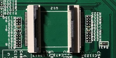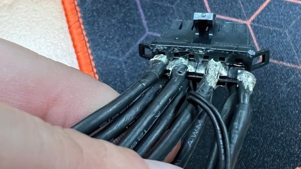
showing the connector after its torn down from the side of the wire solder points, showing how thin are the metal pads, and also that one wire has already broken off

NVIDIA Power Cables Are Melting, This May Be Why

NVIDIA has recently released their lineup of 40-series graphics cards, with a novel generation of power connectors called 12VHPWR. See, the previous-generation 8-pin connectors were no longer enough to satiate the GPU’s hunger. Once cards started getting into the hands of users, surprisingly, we began seeing pictures of melted 12VHPWR plugs and sockets online — specifically, involving ATX 8-pin GPU power to 12VHPWR adapters that NVIDIA provided with their cards.

Now, [Igor Wallossek] of igor’sLAB proposes a theory about what’s going on, with convincing teardown pictures to back it up. After an unscheduled release of plastic-scented magic smoke, one of the NVIDIA-provided connectors was destructively disassembled. Turned out that these connectors weren’t crimped like we’re used to, but instead, the connectors had flat metal pads meant for wires to solder on. For power-carrying connectors, there are good reasons this isn’t the norm. That said, you can make it work, but chances are not in favor of this specific one.
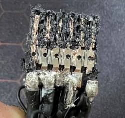
The metal pads in question seem to be far too thin and structurally unsound, as one can readily spot, their cross-section is dwarfed by the cross-section of cables soldered to them. This would create a segment of increased resistance and heat loss, exacerbated by any flexing of the thick and unwieldy cabling. Due to the metal being so thin, the stress points seem quite flimsy, as one of the metal pads straight up broke off during disassembly of the connector.

If this theory is true, the situation is a blunder to blame on NVIDIA. On the upside, the 12VHPWR standard itself seems to be viable, as there are examples of PSUs with native 12HPWR connections that don’t exhibit this problem. It seems, gamers with top-of-the-line GPUs can now empathize with the problems that we hackers have been seeing in very cheap 3D printers.
M.2 For Hackers – Expand Your Laptop

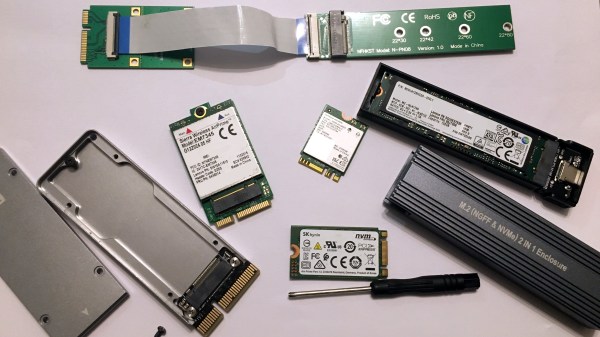
You’ve seen M.2 cards in modern laptops already. If you’re buying an SSD today, it’s most likely an M.2 one. Many of our laptops contain M.2 WiFi cards, the consumer-oriented WWAN cards now come in M.2, and every now and then we see M.2 cards that defy our expectations. Nowadays, using M.2 is one of the most viable ways for adding new features to your laptop. I have found that the M.2 standard is quite accessible and also very hackable, and I would like to demonstrate that to you.

If you ever searched the Web trying to understand what makes M.2 tick, you might’ve found one of the many confusing articles which just transcribe stuff out of the M.2 specification PDF, and make things look more complicated than they actually are. Let’s instead look at M.2 real-world use. Today, I’ll show you the M.2 devices you will encounter in the wild, and teach you what you need to know to make use of them. In part 2, I will show you how to build your own M.2 cards and card-accepting devices, too!

Well Thought-Out, Mostly

You can genuinely appreciate the M.2 standard once you start looking into it, especially if you have worked with mPCIe devices for some amount of time. mPCIe is what we’ve been using for all these years, and it gradually became a mish-mash of hardly-compatible pinouts. As manufacturers thought up all kinds of devices they could embed, you’d find hacks like mSATA and WWAN coexistence extensions, and the lack of standardization is noticeable in things like mPCIe WWAN modems as soon as you need something like UART or PCM. The M.2 specification, thankfully, accounted for all of these lessons.

Continue reading “M.2 For Hackers – Expand Your Laptop” →

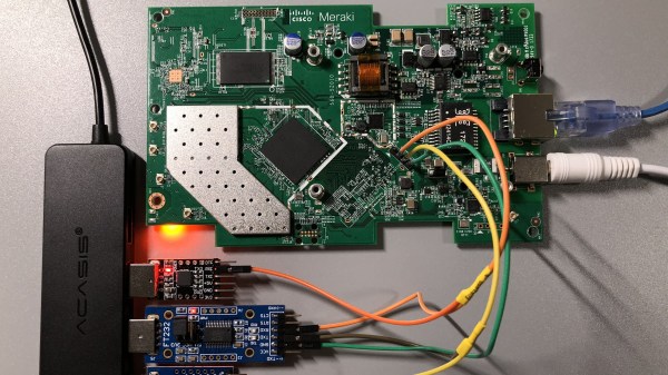
The Meraki AP PCB on a desk, case-less, with three USB-UARTs connected to its pins - one for interacting with the device, and two for monitoring both of the UART data lines.

Flashing Booby-Trapped Cisco AP With OpenWrt, The Hard Way

Certain manufacturers seriously dislike open-source firmware for their devices, and this particular hack deals with quite extreme anti-hobbyist measures. The Meraki MR33, made by Cisco, is a nice access point hardware-wise, and running OpenWrt on it is wonderful – if not for the Cisco’s malicious decision to permanently brick the CPU as soon as you enter Uboot through the serial port. This AP seems to be part of a “hardware as a service” offering, and the booby-trapped Uboot was rolled out by an OTA update some time after the OpenWrt port got published.

There’s an older Uboot version available out there, but you can’t quite roll back to it and up to a certain point, there was only a JTAG downgrade path noted on the wiki – with its full description consisting of a “FIXME: describe the process” tag. Our hacker, an anonymous user from the [SagaciousSuricata] blog, decided to go a different way — lifting, dumping and modifying the onboard flash in order to downgrade the bootloader, and guides us through the entire process. There’s quite a few notable things about this hack, like use of Nix package manager to get Python 2.7 on an OS which long abandoned it, and a tip about a workable lightweight TFTP server for such work, but the flash chip part caught our eye.

The flash chip is in TSOP48 package and uses a parallel interface, and an iMX6.LL devboard was used to read, modify and flash back the image — hotswapping the chip, much like we used to do with old parallel-interface BIOS chips. We especially liked the use of FFC cables and connectors for connecting the flash chip to the devboard in a way that allows hotswapping – now that we can see it, the TSOP 0.5 mm pitch and 0.5 mm FFC hardware are a match made in heaven. This hack, of course, will fit many TSOP48-equipped devices, and it’s nice to have a toolkit for it in case you don’t have a programmer handy.
In the end, the AP got a new lease of life, now governed by its owner as opposed to Cisco’s whims. This is a handy tutorial for anyone facing a parallel-flash-equipped device where the only way appears to be the hard way, and we’re glad to see hackers getting comfortable facing such challenges, whether it’s parallel flash, JTAG or power glitching. After all, it’s great when your devices can run an OS entirely under your control – it’s historically been that you get way more features that way, but it’s also that the manufacturer can’t pull the rug from under your feet like Amazon did with its Fire TV boxes.

We thank [WifiCable] for sharing this with us!

(Ed Note: Changed instances of “OpenWRT” to “OpenWrt”.)

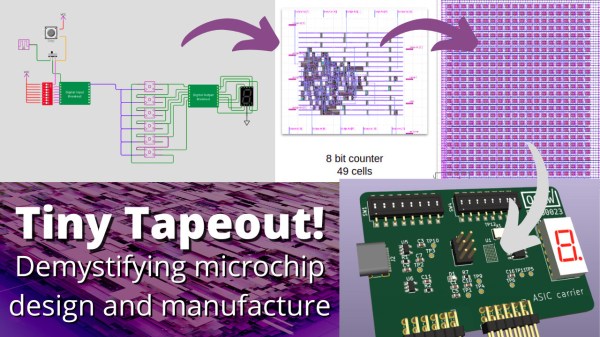
A sequence of pictures with arrows between each other. This picture shows a Wokwi (Fritzing-like) diagram with logic gates, going to a chip shot, going to a panel of chipsGA footprint on a KiCad PCB render with DIP switches and LEDs around the breakout. Under the sequence, it says: "Tiny Tapeout! Demystifying microchip design and manufacture"

Design Your Own Chip With TinyTapeout

When hackers found and developed ways to order PCBs on the cheap, it revolutionized the way we create. Accessible 3D printing brought us entire new areas to create things. [Matt Venn] is one of the people at the forefront of hackers designing our own silicon, and we’ve covered plenty of his research over the years. His latest effort to involve the hacker community, TinyTapeout, makes chip design accessible to newcomers – the bar is as low as arranging logic gates on a web browser page.

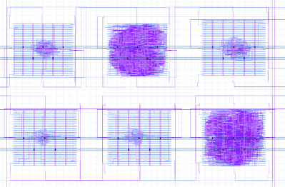
Six chip shots shown, with various densities of gates being used - some use a little, and some use a the entire area given.
Just six of the designs submitted, with varying complexity

For this, [Matt] worked with people like [Uri Shaked] of Wokwi fame, [Sylvain “tnt” Munaut], [jix], and a few others. Together, they created all the tooling necessary, and most importantly, a pipeline where your logic gate-based design in Wokwi gets compiled into a block ready to be put into silicon, with even simulations and compile-time verification for common mistakes. As a result, the design process is remarkably straightforward, to the point where a 9-year-old kid can do it. If you wanted, you could submit your Verilog, too!

The first round of TinyTapeout had a deadline in the first days of September and brought 152 entries together – just in time for an Efabless shuttle submission. All of these designs were put on a single instance of a chip, that will be fabbed in quantity, tested, soldered onto breakouts, and mailed out to individual participants. In this way, everyone will be getting everyone’s design, but thanks to the on-chip muxing hardware, they’re able to switch between designs using on-breakout DIP switches.

More after the break…

Continue reading “Design Your Own Chip With TinyTapeout” →

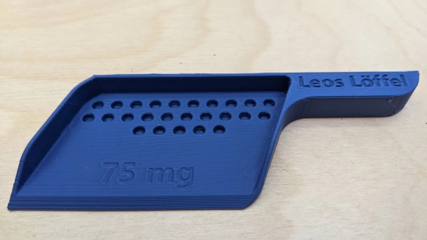
The dosing spoon shown, with many round openings for medication pellets to go into

Medicine Dosing Spoon Discontinued, Made 3D Printable Instead

[Gregor Herz] caught wind of a problem that neuropediatric clinics in Germany have been facing recently. Orfiril, a seizure-preventing medication used in those clinics for treating children, is normally prescribed to adults, and the usual dosages are too high for kids. Orfiril comes in regular pill-shaped capsules, each capsule containing a bunch of small medication-soaked pellets, and you only need a certain amount of these pellets if you want to achieve a lower dose.

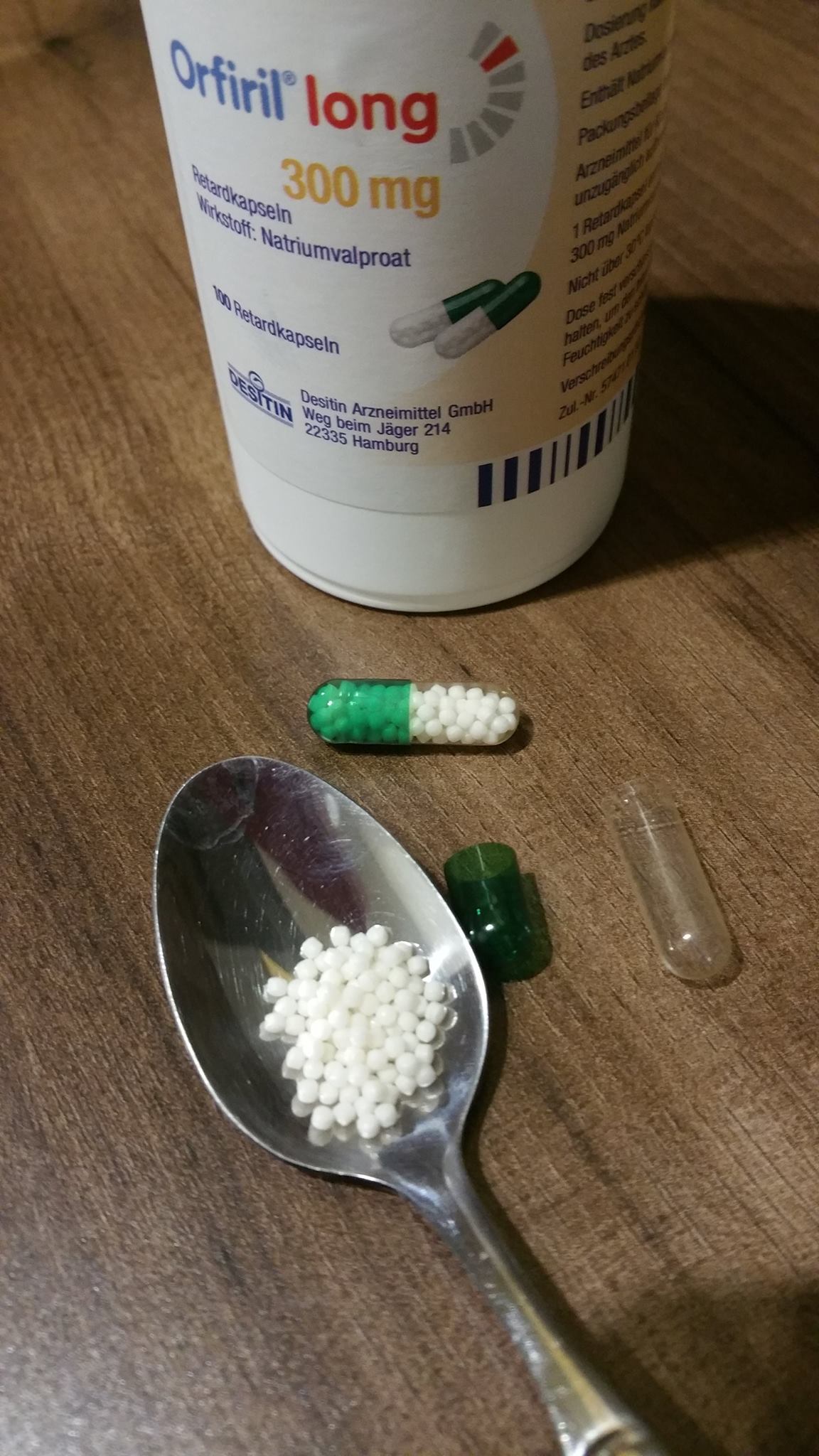
An Orfiril medication bottle is shown, with an Orfiril pill capsule next to it, showing the small pellets inside. Another pill capsule has been disassembled, with the pellets inside a teaspoon.It used to be that you could get a special spoon helping you to get a proper dosage — but sadly, the original supplier has quit making these. So, our hacker designed a 3D printable model instead.

[Gregor] tells us that a lot of clinics in Germany are facing this exact issue right now, so sharing this model may mean that more hospitals can work around the supply issue. Provided a friendly hobbyist has food-grade 3D printing conditions available, anyway. He tells about some suitable filaments models you can buy, as well as research on food-grade printing requirements — a topic we’ve talked about in detail, and just this month have seen someone revisit with reassuring results. Are you interested in printing some of these? If so, there might be a clinic nearby that’d be thankful.

We’ve seen a surge of 3D printing for medical uses two years ago, back when supply chain issues had doctors face PPE shortages, and some critical parts for equipment were in short supply. Before that, we’d sometimes see medical purpose 3D printing done in dire circumstances, when no other choices were available. Now 3D printing of medical devices is more accepted, and we can’t wait for more research and hacking on this front!

front and back of the Jolly Wrencher SAO

Jolly Wrencher SAO, And How KiCad 6 Made It Easy

If you plan to attend Supercon or some other hacker conference, know that you’re going to get a badge with a SAO (Simple Add-On) connector, a 4-pin or 6-pin connector that you can plug an addon board onto. There’s myriads of SAOs to choose from, and if you ever felt like your choice paralysis wasn’t intense enough, now you have the option of getting a Jolly Wrencher SAO board!

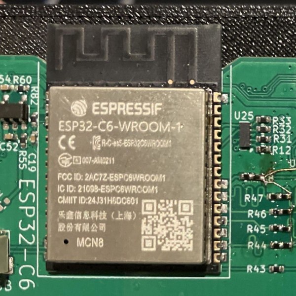
This board gives you an SMD prototyping space, with 1.27mm (0.05″ pitch) pads, suitable for many passive components, ICs and even modules like the ESP32 WROOM. Those pads are diagonally interspersed with ground-fill-connected pads – if you want to bodge something on the spot, you don’t need to pull separate GND wires. Given the Supercon badge specifics, the SAO-standard SDA and SCL pins have RX and TX labels as well. For bonus points, the eyes are transparent, with LED footprints behind them – it’s my first time designing a PCB where the LED shines through the FR4, and I hope that the aesthetics work out!

This design is open with gerber files available for download, so if you thought of making a quick PCB order, I’m giving you one more .zip file to add to it. Otherwise, it’s possible that you will find a Wrencher board lying around at Supercon! Now, I’d like to tell you how KiCad 6 made it super easy to design this PCB – after all, there’s never enough SAOs, and it’s quite likely you’ll want to design your own special SAO, too.

Continue reading “Jolly Wrencher SAO, And How KiCad 6 Made It Easy” →

Lithium-Ion Battery Circuitry Is Simple

By now, we’ve gone through LiIon handling basics and mechanics. When it comes to designing your circuit around a LiIon battery, I believe you could benefit from a cookbook with direct suggestions, too. Here, I’d like to give you a collection of LiIon recipes that worked well for me over the years.

I will be talking about single-series (1sXp) cell configurations, for a simple reason – multiple-series configurations are not something I consider myself as having worked extensively with. The single-series configurations alone will result in a fairly extensive writeup, but for those savvy in LiIon handling, I invite you to share your tips, tricks and observations in the comment section – last time, we had a fair few interesting points brought up!

The Friendly Neighborhood Charger

There’s a whole bunch of ways to charge the cells you’ve just added to your device – a wide variety of charger ICs and other solutions are at your disposal. I’d like to focus on one specific module that I believe it’s important you know more about.

You likely have seen the blue TP4056 boards around – they’re cheap and you’re one Aliexpress order away from owning a bunch, with a dozen boards going for only a few bucks. The TP4056 is a LiIon charger IC able to top up your cells at rate of up to 1 A. Many TP4056 boards have a protection circuit built in, which means that such a board can protect your LiIon cell from the external world, too. This board itself can be treated as a module; for over half a decade now, the PCB footprint has stayed the same, to the point where you can add a TP4056 board footprint onto your own PCBs if you need LiIon charging and protection. I do that a lot – it’s way easier, and even cheaper, than soldering the TP4056 and all its support components. Here’s a KiCad footprint if you’d like to do that too.

Continue reading “Lithium-Ion Battery Circuitry Is Simple” →