Part of the reason that retrocomputers are still so popular despite their obsolescence is that it’s possible to understand the entire inner workings of a computer like this, from the transistors all the way up to the software. Comparatively, it will likely be a long time (if ever) before anyone is building a modern computer from discrete components. To illustrate this point, plenty of 8-bit computers are available to either restore from original 80s hardware or to build from kits. And if you’d like to get even deeper into the weeds you can design your own computer including the instruction set completely from the ground up using an FPGA.
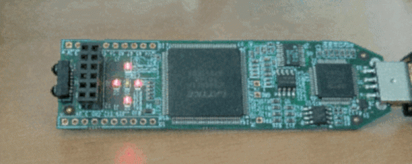
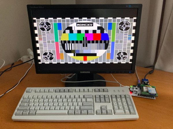
This project, called the Moncky project, is a step above the usual 8-bit computer builds as it is actually a 16-bit computer. It is built around an Arty Spartan-7 FPGA dev board running around 20 MHz and has access to 2 x 128 kB dual-port RAM for memory. To access the outside world there is a VGA output, PS/2 capability, SPI, and uses an SD card as a hard drive. This project really shines in the software, though, as the project creator [Kris Demuynck] builds everything from scratch in order to illustrate how everything works for educational purposes, and is currently working on implementing a C compiler to make programming the computer easier.
All of the project files, as well as all of the code, are available on the project’s GitHub page if you’d like to follow along or build on this homebrew 16-bit computer. It’s actually the third iteration of this computer, with the Moncky-1 and Moncky-2 being used to develop the more basic building blocks for this computer. While it’s not the first 16-bit computer we’ve seen implemented on an FPGA, it is one of the few that builds its own RISC instruction set and associated software rather than cloning a known existing processor. We’ve also seen some interesting x86 implementations on an FPGA as well.
Thanks to [koen-ieee] for the tip!