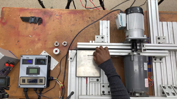
The Mostly Printed CNC (MPCNC) is an impressive project in its own right, allowing anyone with a 3D printer and some electrical conduit to build their own fairly heavy-duty CNC platform perfect for routing. Customization is the name of the game with the MPCNC, and few machines will look the same when they’re done. But even fewer will feature a control interface nearly as slick as the wireless handset that [Steve Croot] has put together for his.
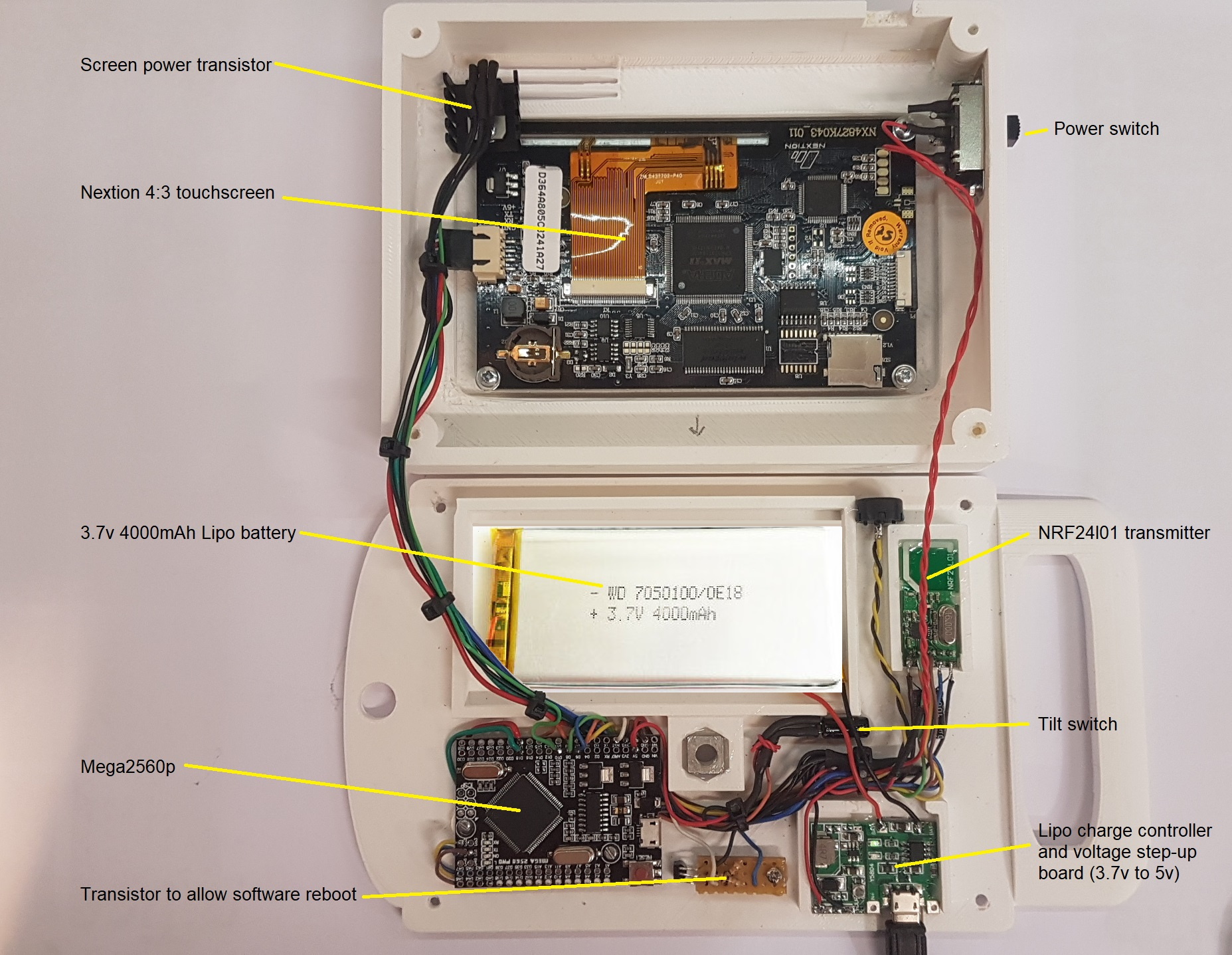 On the hardware side, the project is fairly straightforward. Inside the 3D printed enclosure is a 4.3″ Nextion touchscreen, a Mega 2560 PRO microcontroller, a nRF24L01 2.4 GHz transceiver, and a 4000 mAh 3.7 V LiPo battery with appropriate charging circuit. Besides the physical toggle switch to turn the handheld on and off, all of the device’s functions are touch controlled. For the receiver side, [Steve] is using another nRF24L01 radio and microcontroller pair to toggle relays and shuffle the appropriate G-code commands around.
But what really makes this project shine is the software. As you can see in the video after the break, [Steve] has done an absolutely phenomenal job with the user interface on this controller. The themed boot screen and concise iconography give the controller a very professional look, and the ability to jog the machine around using taps on a virtual workspace helps keep the touch interface from being a gimmick.
We’ve seen some impressive custom-built CNC controllers over the years, but between the mostly off-the-shelf hardware used and impressive UI, we think [Steve] has created something unique. It looks like he’s keeping the source code to himself for the time being, but hopefully he sees fit to release it in the future; a project of this caliber deserves to become more than a one-off creation.
Continue reading “A Wireless Controller For The Mostly Printed CNC”