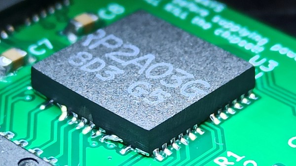
You can achieve a lot with a Dremel. For instance, apparently you can slim the original NES down into the hand-held form-factor. Both the CPU and the PPU (Picture Processing Unit) are 40-pin DIP chips, which makes NES minification a bit tricky. [Redherring32] wasn’t one to be stopped by this, however, and turned these DIP chips into QFN-style-mounted dies (Nitter) using little more than a Dremel cutting wheel. Why? To bring his TinyTendo handheld game console project to fruition, of course.
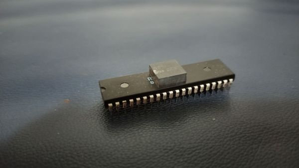
DIP chip contacts go out from the die using a web of metal pins called the leadframe. [Redherring32] cuts into that leadframe and leaves only the useful part of the chip on, with the leadframe pieces remaining as QFN-like contact pads. Then, the chip is mounted onto a tailored footprint on the TinyTendo PCB, connected to all the other components that are, thankfully, possible to acquire in SMD form nowadays.
This trick works consistently, and we’re no doubt going to see the TinyTendo being released as a standalone project soon. Just a year ago, we saw [Redherring32] cut into these chips, and wondered what the purpose could’ve been. Now, we know: it’s a logical continuation of his OpenTendo project, a mainboard reverse-engineering and redesign of the original NES, an effort no doubt appreciated by many a NES enthusiast out there. Usually, people don’t cut the actual chips down to a small size – instead, they cut into the mainboards in a practice called ‘trimming’, and this practice has brought us many miniature original-hardware-based game console builds over these years.
As the world begins to slowly pull itself out of the economic effects of the pandemic, there’s one story that has been on our minds for the past couple of years, and it’s probably on yours too. The chip shortage born during those first months of the pandemic has remained with us despite the best efforts of the industry. Last year, pundits were predicting a return to normality in 2022, but will unexpected threats to production such as the war in Ukraine keep us chasing supplies? It’s time to delve into the root of the issue and get to the bottom of it for a Hackaday report.
The Chips Are Down
Consumers were more interested in toilet paper than chip supply during the lockdown.
Going back to 2020, and as global economies abruptly slowed down in the face of stringent lockdowns it’s clear that both chipmakers and their customers hugely underestimated the effect that the pandemic would have on global demand for chips.
As production capacity was reduced or turned to other products in response to the changed conditions, it was soon obvious that the customers’ hunger for chips had not abated, resulting in a shortfall between supply and demand.
We’ve all experienced the chaos that ensued as the supply of popular varieties dried up almost overnight, and as fresh pandemic waves have broken around the world along with a crop of climate and geopolitical uncertainties it’s left many wondering whether the chip situation will ever be the same again.
Green Shoots In Idaho
Idaho leads the way in a chip shortage recovery! inkknife_2000, CC BY-SA 2.0
Amidst all that gloom, there are some encouraging green shoots to be seen. While it’s perhaps not quite time to celebrate, there’s a possibility for some cautious optimism. This month brought the hope that Potato Semiconductor might be cutting the sod on a new production capacity for their ultra-fast digital logic in Idaho, and with other manufacturers following suit it could be that we’ll once again have all the chip capacity we can eat.
But the other side of the chip business coin lies with the customer: we all see the chip shortage from our own semi-insider perspective, but have the tastes of the general public returned towards chips? Early signs are that as consumer confidence returns there are encouraging trends in chip consumption taking root, so we’d be inclined to advise our readers to have cautious optimism. If all goes well, you’ll be having your chips by summer.
The prospects for a new dawn in chip production capacity in 2022 look rosy, but there’s a further snag on the horizon courtesy of the Russian invasion of Ukraine. Like so many industries in a globalised economy, the chip industry depends heavily on supplies, consumables, and machinery from beyond the borders of wherever the plants themselves may lie.
In the case of Ukraine there’s a particular raw material whose supply has been severely interrupted, and though we hope for a speedy resolution of the conflict and a consequent resumption of production, the knock-on effect on the production of chips in the rest of the world can not be underestimated. Despite the ramp-up in output led by Idaho, the production of chips globally still relies heavily on Ukrainian sunflower oil. There’s a possibility that an acceptable substitute might be found in canola oil, but it will remain to be seen whether the chip-eating consumers will notice the taste difference.
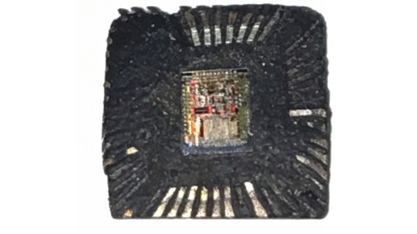
At least by today’s standards, some of the early chips were really, really big. They may have been revolutionary and they certainly did shrink the size of electronic devices, but integrating a 40-pin DIP into a modern design can be problematic. The solution: cut off all the extra plastic and just work with the die within.
When you buy a chip, how can you be sure you’re getting what you paid for? After all, it’s just a black fleck of plastic with some leads sticking out of it, and a few laser-etched markings on it that attest to what lies within. All of that’s straightforward to fake, of course, and it’s pretty easy to tell if you’ve got a defective chip once you try it out in a circuit.
But what about off-brand chips? Those chips might be functionally similar, but still off-spec in some critical way. That was the case for [Kevin Darrah] which led to his forensic analysis of potentially counterfeit MCU chips. [Kevin] noticed that one of his ATMega328 projects was consuming way too much power in deep sleep mode — about two orders of magnitude too much. The first video below shows his initial investigation and characterization of the problem, including removal of the questionable chip from the dev board it was on and putting it onto a breakout board that should draw less than a microamp in deep sleep. Showing that it drew 100 μA instead sealed the deal — something was up with the chip.
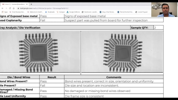
[Kevin] then sent the potentially bogus chip off to a lab for a full forensic analysis, because of course there are companies that do this for a living. The second video below shows the external inspection, which revealed nothing conclusive, followed by an X-ray analysis. That revealed enough weirdness to warrant destructive testing, which showed the sorry truth — the die in the suspect unit was vastly different from the Atmel chip’s die.
It’s hard to say that this chip is a counterfeit; after all, Atmel may have some sort of contract with another foundry to produce MCUs. But it’s clearly an issue to keep in mind when buying bargain-basement chips, especially ones that test functionally almost-sorta in-spec. Caveat emptor.
Counterfeit parts are depressingly common, and are a subject we’ve touched on many times before. If you’d like to know more, start with a guide.
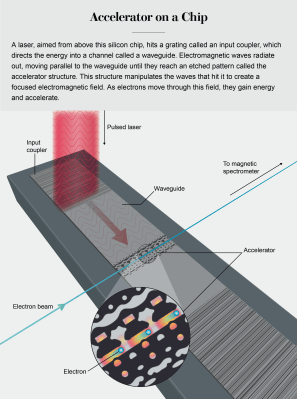
If you were asked to imagine a particle accelerator, you would probably picture a high-energy electron beam contained within a kilometers-long facility, manned by hundreds of engineers and researchers. You probably wouldn’t think of a chip smaller than a fingernail, yet that’s exactly what the SLAC National Accelerator Laboratory’s Accelerator on a Chip International Program (ACHIP) has accomplished.
The Stanford University team developed a device that uses lasers to accelerate electrons along etched channels on a silicon chip. The idea for a miniature accelerator has existed since the laser’s invention in 1960, but the requirement for a device to generate electrons made the early proof-of-concepts difficult to manufacture in bulk.
via Scientific American
The electromagnetic waves produced by lasers have much shorter wavelengths than the microwaves used in full-scale accelerators, allowing them to accelerate electrons in a far more confined space – channels can be shrunk to three one-thousandths of a millimeter wide. In order to couple the lasers and electrons properly, the light waves must push the particles in the correct direction with as much energy as possible. This also requires the device to generate electrons and transmit them via the proper channel. With an accelerator engraved in silicon, multiple components can fit on the same chip.
Within the latest prototype, a laser hits a grating from above the chip, directing the energy into a waveguide. The electromagnetic waves radiate out, moving with the waveguide until they reach an etched pattern that creates a focused electromagnetic field. As electrons move through the field, they accelerate and gain energy.
The results showed that the prototype could boost the electrons by 915 electron volts, equivalent to the electrons gaining 30 million electron volts over a meter. While the change is not on the scale of SLAC, it does scale up more easily since researchers can fit multiple accelerating paths onto future designs without the bulk of a full-scale accelerator. The chip exists as a single stage of the accelerator, allowing more researchers to conduct experiments without the need to reserve space in expensive full-scale particle accelerators.
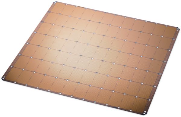
We get it, press releases are full of hyperbole. Cerebras recently announced they’ve built the largest chip ever. The chip has 400,000 cores and contains 1.2 trillion transistors on a die over 46,000 square mm in area. That’s roughly the same as a square about 8.5 inches on each side. But honestly, the WSE — Wafer Scale Engine — is just most of a wafer not cut up. Typically a wafer will have lots of copies of a device on it and it gets split into pieces.
According to the company, the WSE is 56 times larger than the largest GPU on the market. The chip boasts 18 gigabytes of storage spread around the massive die. The problem isn’t making such a beast — although a normal wafer is allowed to have a certain number of bad spots. The real problems come through things such as interconnections and thermal management.
There can be few of us who haven’t gazed with fascination upon the work of IC decappers, whether they are showing us classic devices from the early years of mass semiconductor manufacture, or reverse-engineering the latest and greatest. But so often their work appears to require some hardcore scientific equipment or particularly dangerous chemicals. We’ve never thought we might be able to join the fun. [Generic Human] is out to change all that, by decapping chips using commonly available chemicals and easy to apply techniques. In particular, we discover through their work that rosin — the same rosin whose smell you will be familiar with from soldering flux — can be used to dissolve IC packaging.
Of course, ICs that dissolved easily in the face of soldering wouldn’t meet commercial success, so an experiment with flux meets little success. Pure rosin, however, appears to be an effective decapping agent. [Generic Human] shows us a motherboard voltage regulator boiled in the stuff. When the rosin is removed with acetone, there among the debris is the silicon die, reminding us just how tiny these things are. We’re sure you’ll all be anxious to try it for yourselves, now, so take a while to look at the video below showing their CCC Congress talk.
The master of chip decapping is of course [Ken Shirriff], whose work we’ve featured many times. Our editor [Mike Szczys] interviewed him last year, and it’s well worth a look.