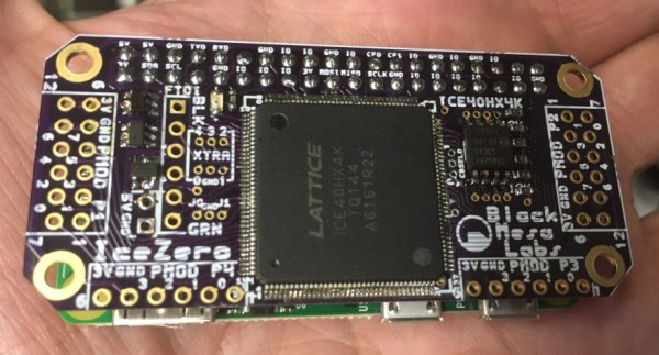
Every year, new models of laptops arrive on the shelves. This means that old laptops usually end up in landfills, which isn’t exactly ideal. If you don’t want to waste an old or obsolete laptop, though, there’s a way to reuse at least the screen out of one. Simply grab an FPGA off the shelf and get to work.
[Martin] shows us all how to perform this feat on our own, and goes into great detail about how all of the electronics involved work. Once everything was disassembled and the FPGA was wired up, it took him a substantial amount of time just to turn the display on. From there it was all downhill: [Martin] can now get any pattern to show up on the screen, within reason. The only limit to his display now seems to be the lack of external RAM. He currently uses the setup to drive an impressive-looking clock.
This is a big step from days passed where it was next to impossible to repurpose a laptop screen. Eventually someone discovered a way to drive these displays, and now there are cheap electronics from China that can usually get a screen like this running. It’s impressive to see it done from scratch, though, and the amount of detail in the videos are a great way to understand how everything is working.
For humans, moving our arms and hands onto an object to pick it up is pretty easy; but for manipulators, it’s a different story. Once we’ve found the object we want our robot to pick up, we still need to plan a path from our robot hand to the object all the while lugging the remaining limbs along for the ride without snagging them on any incoming obstacles. The space of all possible joint configurations is called the “joint configuration space.” Planning a collision-free path through them is called path planning, and it’s a tricky one to solve quickly in the world of robotics.
These days, roboticists have nailed out a few algorithms, but executing them takes 100s of milliseconds to compute. The result? Robots spend most of their time “thinking” about moving, rather than executing the actual move.
Robots have been lurching along pretty slowly for a while until recently when researchers at Duke University [PDF] pushed much of the computation to hardware on an FPGA. The result? Path planning in hardware with a 6-degree-of-freedom arm takes under a millisecond to compute!
It’s worth asking: why is this problem so hard? How did hardware make it faster? There’s a few layers here, but it’s worth investigating the big ones. Planning a path from point A to point B usually happens probabilistically (randomly iterating to the finishing point), and if there exists a path, the algorithm will find it. The issue, however, arises when we need to lug our remaining limbs through the space to reach that object. This feature is called the swept volume, and it’s the entire shape that our ‘bot limbs envelope while getting from A to B. This is not just a collision-free path for the hand, but for the entire set of joints.
Image Credit: Robot Motion Planning on a Chip
Encoding a map on a computer is done by discretizing the space into a sufficient resolution of 3D voxels. If a voxel is occupied by an obstacle, it gets one state. If it’s not occupied, it gets another. To compute whether or not a path is OK, a set of voxels that represent the swept volume needs to be compared against the voxels that represent the environment. Here’s where the FPGA kicks in with the speed bump. With the hardware implementation, voxel occupation is encoded in bits, and the entire volume calculation is done in parallel. Nifty to have custom hardware for this, right?
We applaud the folks at Duke University for getting this up-and-running, and we can’t wait to see custom “robot path-planning chips” hit the market some day. For now, though, if you’d like to sink your teeth into seeing how FPGAs can parallelize conventional algorithms, check out our linear-time sorting feature from a few months back.
[Bunnie Huang] and [Edward Snowden] have teamed up to publish a paper exploring the possibility of introspection on the iPhone.
A rendering of the proposed introspection device attached to an iPhone6
The idea is that phones are increasingly complex and potentially vulnerable to all kinds of digital surveillance. Even airplane mode is insufficient for knowing that your phone isn’t somehow transmitting information. The paper looks at the various radios on the iPhone, going so far as opening up the device and reading signals at each of the chips for cell, WiFi, Bluetooth, GPS, and NFC to determine whether the chip itself is doing anything, regardless of what the screen says. This introspection can then be used to be confident that the phone is not communicating when it shouldn’t be.
The paper goes on to propose a device that they will prototype in the coming year which uses an FPC that goes into the phone through the SIM card port. It would contain a battery, display, buttons, multiple SIM cards, and an FPGA to monitor the various buses and chips and report on activity.
Significant hacking of an iPhone will still be required, but the idea is to increase transparency and be certain that your device is only doing what you want it to.
Any maker worth their bits will look for new ways to challenge themselves. [Robert Fotino], a computer science student at the University of California, is doing just that: designing and building his own lightweight hobbyist game console that he has appropriately named Consolite.
[Fotino] wrote his own compiler in C++ that converts from C-like languages to a custom-designed assembler that he has dubbed Consolite Assembly. To test his code, he also wrote an emulator before loading it onto the Mimas V2 FPGA board. Presently, Consolite uses 64KiB of main memory and 48 KiB of video memory; a future version will have 32 bit support to make better use of the Mimas’ 64 MiB of on board ram, but the current 16-bit version is a functional proof of concept.
An SD card functions as persistent storage for up to 256 programs, which can be accessed using the hardware switches on the Mimas, with plans to add user access in the form of saving game progress, storage outside of main memory, etc. — also in a future update that will include audio support.
As it stands, [Fotino] has written his own versions of Breakout, Tetris, and Tron to show off his project.
Not wanting for diligence, [Fotino] has provided thorough documentation of nearly every step along the way in his blog posts and on GitHub if you are looking for guidelines for any similar projects you might have on the back burner — like an even tinier game console.
One day [Andy] was cruising around eBay and spotted something interesting. Forty Virtex-E FPGAs for two quid each. These are the big boys of the FPGA world, with 512 user IO pins, almost 200,000 logic gates, packed into a 676-ball BGA package. These are not chips designed for the hobbyist. These chips are not designed for boards with less than six layers. These chips aren’t even designed for boards with 6/6mil tolerances from the usual suspects in China. By any account, a 676-ball package is not like a big keep out sign for hobbyists. You don’t turn down a £2 class in advanced PCB design, though, leading to one of the most impressive ‘I just bought some crap on eBay’ projects we’ve seen.
The project [Andy] had in mind for these chips was a generic dev board, which meant breaking out the IO pins and connecting some SRAM, SDRAM, and Flash memory. The first issue with this project is escape routing all the balls. Xilinx published a handy application note that recommends specific design parameters for the traces of copper under the chip. Unfortunately, this was a six-layer board, and the design rules in the application note were for 5/5mil traces. [Andy]’s board house can’t do six-layer boards, and their design rules are for 6/6mil traces. To solve this problem, [Andy] just didn’t route the inner balls, and hoped the 5mil traces would work out.
With 676 tiny little pads on a PCB, the clocks routed, power supply implemented, too many decoupling caps on the back, differential pairs, static RAM, a few LEDs placed just for fun, [Andy] had to solder this thing up. Since the FPGA was oddly one of the less expensive items on the BOM, he soldered that first, just to see if it would work. It did, which meant it was time to place the RAM, Flash, and dozens of decoupling caps. Everything went relatively smoothly – the only problem was the tiny 0402 decoupling caps on the back of the board. This was, by far, the hardest part of the board to solder. [Andy] only managed to get most of the decoupling caps on with a hot air gun. That was good enough to bring the board up, but he’ll have to figure some other way of soldering those caps for the other 30 or so boards.
Slowly, very slowly, the time when we don’t subject embedded beginners to AVRs and PICs is coming. At a glacial pace, FPGA development platforms are becoming ever more capable and less expensive. [Eric Brombaugh] has been playing around with both ARMs and FPGAs for a while now and decided to combine these two loves into a single board that’s capable of a lot.
This board is fittingly called an STM32F303 + ice5 development board, and does exactly what it says on the tin. There’s an STM32F303 on board providing a 32-bit CPU running at 72 MHz, 48 kB of SRAM, a quarter meg of Flash, and enough peripherals to keep anyone happy. The FPGA side of this board is a Lattice iCE5 with about 3k Look Up Tables (LUTs), and one time programmable non-volatile config memory.
The connections between the ARM and FPGA include a dedicated SPI port, and enough GPIOs to implement full-duplex I2S and a USART. Like all good projects, [Eric] has shared all the files, schematics, and BOMs required to make this board your very own reality, and has provided a few links to the development toolchains. While the FPGA is from Lattice’s ice40 family, it’s not supported by the Open Source Project Icestorm toolchain. Still, it’s a very capable board for ARM and FPGA development.
To decode the device’s packets he reached for his RTL-SDR receiver and took a look at it in software. GQRX confirmed the presence of the carrier and allowed him to record a raw I/Q file, which he could then supply to Inspectrum to analyse the packet structure. He found it to be a simple on-off keying scheme, with bits expressed through differing pulse widths. He was then able to create a Gnu Radio project to read and decode them in real time.
Emulating the transmitter was then a fairly straightforward process of generating a 350MHz clock using the on-board PLL and gating it with his generated data stream to provide modulation. The result was able to control his fan with a short wire antenna, indeed he was worried that it might also be doing so for other similar fans in his apartment complex. You can take a look at his source code on GitHub if you would like to try something similar.
It’s worth pointing out that a transmitter like this will radiate a significant amount of harmonics at multiples of its base frequency, and thus without a filter on its output is likely to cause interference. It will also be breaking all the rules set out by whoever the spectrum regulator is where you live, despite its low power. However it’s an interesting project to read, with its reverse engineering and slightly novel use of an FPGA.