Building Diode And Diode-Transistor Logic Gates

AND gate implemented as diode-resistor logic. (Credit: Anthony Francis-Jones)

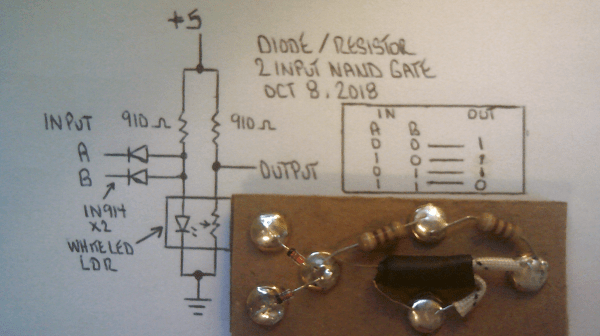
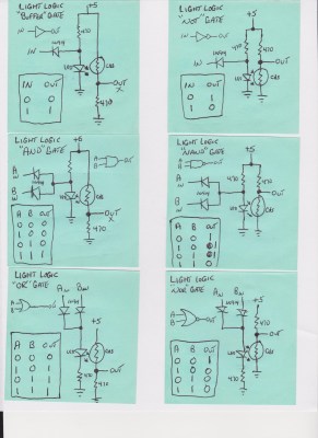
The fun part about logic gates is that there are so many ways to make them, with each approach having its own advantages and disadvantages. Although these days transistor-transistor logic (TTL) is the most common, diode-transistor logic (DTL) once was a regular sight, as well as diode-resistor logic (DRL). These logic gates are the topic of a recent video by [Anthony Francis-Jones], covering a range of logic gates implemented using mostly diodes and resistors.

Of note is that there’s another class of logic gates: this uses resistors and transistors (RTL) and preceded DTL. While DRL can be used to implement AND and OR logic gates, some types of logic gates (e.g. NOT) require an active (transistor) element, which is where DTL comes into play.

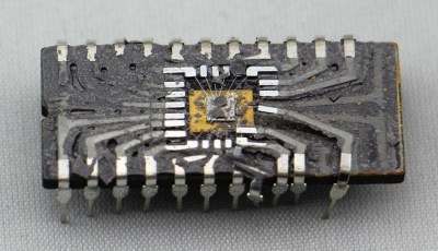
In addition to the construction of a rather nifty demonstration system and explanation of individual logic gates, [Anthony] also shows off a range of DTL cards used in the Bendix G-15 and various DEC systems. Over time TTL would come to dominate as this didn’t have the diode voltage drop and other issues that prevented significant scaling. Although the rise of VLSI has rendered DRL and DTL firmly obsolete, they still make for a fascinating teaching moment and remind us of the effort over the decades to make the computing device on which you’re reading this possible.

Continue reading “Building Diode And Diode-Transistor Logic Gates”

Logic Gate Game Is Fun AND Educational

How well do you know your logic gates? For their final submission for STEM Projects class, [BKriet] gamified the situation using a Raspberry Pi Pico, some blinkenlights, and a not-insignificant amount of 3D printing. The result is Name! That! Gate!, a fun and educational toy that [BKriet] ultimately donated back to the class (that’s a hot move in our book).

The objective of this game is to figure out which logic gate is being used to make the output shown on the screen, given A, B, and/or C as inputs. There are ten stages to the game, and each correct stage awards the player 14 points, for a perfect score of 140. Although a random gate is loaded for every stage, code ensures that no gate is ever repeated during a single game.

This project is completely open source, so the gate is wide open. Don’t have a 3D printer? Here’s a big set of PCB logic gates, but really, you can make logic gates out of almost anything.

Light Emitting Logic Gates Built From Scratch

What’s the weirdest computer you can think of? This one’s weirder.

[Dr. Cockroach] figured out a way to create an inverting NOT gate from just one LED and two resistors (one being a photo-resistor). The Dr. has since built AND, NAND, OR, NOR, XOR and XNOR gates, as well as a buffer, incorporating light into every logic gate.

Traditional inverters – NOT gates – are already made with diodes (typically not light-emitting), resistors (typically not light-dependent), and bipolar transistors. The challenge was to reduce the number of transistors. The schematic from the very first test shows the slight modifications [Dr. Cockroach] made to incorporate light into the logic gate using a 910 Ohm, output LED, and an LED and LDR in parallel.

The output is initially 4.5V for logic 1 and 1.5V for logic 0. Adding two 1N914 diodes and an AND gate ahead of the inverter create a two-input NAND gate. With the two diodes reversed and a 910 Ohm resistor removed, a NOR gate is created.

The next step was to build a S-R latch using the NAND gates and inverters, which holds some basic memory. From there, with some size reductions, a Master-Slave J-K Flip Flop, similarly using NAND gates and inverters, can be built. The current state of the project is a working sequencer and counter. You can even see a smooth sine wave propagating through the LED chaser, which is typically built with ICs or transistors but in this case is built simply with LEDs, LDRs, resistors, and capacitors.

The upcoming plan is to use the gates to build a processor that only uses diodes, resistors, and capacitors. While it’s probably not going to be nearly as fast as any processors we have today, it should be interesting (and educational!) to be able to visually track the flow of data from one logic gate over to the next. Continue reading “Light Emitting Logic Gates Built From Scratch”

Glimmies, As Logic

[Jacob Christ] writes in with a hack that’s going to be this summer’s fidget spinner. Why? The favourite toy of his youngster’s generation is a Glimmie. And while fidget spinners were useful for, well, spinning, the small animal-like Glimmie seems to have an unexpected property, they can function as logic gates.

They form an optical inverter, in their head is a phototransistor and in their belly an LED which goes on when the head is in the dark. He’s found through experimentation that they can be combined to form an AND gate, and thus a NAND gate with the addition of a further inverter.  Since all logic functions can be made from NAND gates, it should therefore be possible to go as far as to make any device based upon logic, even up to a fully functional computer. He estimates the cost of a single gate at $16.30. A computer would require in the region of 80,000 Glimmies to work, but maybe someone with deep enough pockets will be foolhardy enough to give it a try.

You can see the AND gate in action below complete with camera work from a youngster, and if unexpected logic gates are something that’s caught your attention you can take a look at the battery booster pack logic we brought you a while back.

Continue reading “Glimmies, As Logic”

Living Logic: Biological Circuits For The Electrically Minded

Did you know you can build fundamental circuits using biological methods? These aren’t your average circuits, but they work just like common electrical components. We talk alot about normal silicon and copper circuits ‘roud here, but it’s time to get our hands wet and see what we can do with the power of life!

In 1703, Gottfried Wilhelm Leibniz published his Explication de l’Arithmétique Binaire (translated). Inspired by the I Ching, an ancient Chinese classic, Leibniz established that the principles of arithmetic and logic could be combined and represented by just 1s and 0s. Two hundred years later in 1907, Lee De Forest’s “Audion” is used as an AND gate. Forty years later in 1947, Brattain and H. R. Moore demonstrate their “PNP point-contact germanium transistor” in Bell Labs (often given as the birth date of the transistor). Six years later in 1953, the world’s first transistor computer was created by the University of Manchester. Today, 13,086,801,423,016,741,282,5001 transistors have built a world of progressing connectivity, automation and analysis.

While we will never know how Fu Hsi, Leibniz, Forest or Moore felt as they lay the foundation of the digital world we know today, we’re not completely out of luck: we’re in the midst’s of our own growing revolution, but this one’s centered around biotechnology. In 1961, Jacob and Monod discovered the lac system: a biological analog to the PNP transistor presented in Bell Labs fourteen years earlier. In 2000, Gardner, Cantor, and Collins created a genetic toggle switch controlled by heat and a synthetic fluid bio-analog2. Today, AND, OR, NOR, NAND, and XOR gates (among others) have been successfully demonstrated in academic labs around the world.

But wait a moment. Revolution you say? Electrical transistors went from invention to computers in 6 years, and biological transistors went from invention to toggle button in 40? I’m going to get to the challenges facing biological circuits in time, but suffice it to say that working with living things that want to be fed and (seem to) like to die comes with its own set of challenges that aren’t relevant when working with inanimate and uncaring transistors. But, in the spirit of hacking, let’s dive right in. Continue reading “Living Logic: Biological Circuits For The Electrically Minded”

Relay Computing

Recently, [Manuel] did a post on making logic gates out of anything. He mentioned a site about relay logic. While it is true that you can build logic gates using switch logic (that is, two switches in series are an AND gate and two in parallel are an OR gate), it isn’t the only way. If you are wiring a large circuit, there’s some benefit to having regular modules. A lot of computers based on discrete switching elements worked this way: you had a PCB that contained some number of a basic gate (say, a two input NAND gate) and then the logic was all in how you wired them together. And in this context, the SPDT relay was used as a two input multiplexer (or mux).

In case you think the relay should be relegated to the historical curiosity bin, you should know there are still applications where they are the best tool for the job. If you’re not convinced by normal macroscopic relays, there is some work going on to make microscopic relays in ICs. And even if they don’t use relays to do it, some FPGAs use mux-based logic inside.  So it’s worth your time to dig into the past and see how simply switching between two connections can make a computer.

Mux Mania

How do you go from a two input mux to an arbitrary logic gate? Simple, if you paid attention to the banner image. (Or try it interactive). The mux symbols show the inputs to the left, the output to the right and the select input at the bottom. If the select is zero, the “0” input becomes the output. If the select is one, the “1” input routes to the output.

Continue reading “Relay Computing”

Yes, You Can Reverse Engineer This 74181

[Ken Shirriff] is the gift that keeps on giving this new year. His latest is a reverse engineering of the 74181 Arithmetic Logic Unit (ALU). The great news is that the die image and complexity are both optimized for you to succeed at doing your own reverse engineering.

74181-openedWe have most recently seen [Ken] at work explaining his decapping and reverse engineering process at the Hackaday SuperCon followed soon after by his work on the 8008. That chip is crazy with complexity and a die-ogling noob (like several of us on the Hackaday crew) stands no chance of doing more than simply following along with what he explains. This time around, the 74181 is just right for the curious but not obsessed. Don’t believe me? The 8008 had around 3,500 transistors while the friendly 74181 hosts just 170. We like those odds!

A quick crash course in visually recognizing transistors will have you off to the races. [Ken] also provides reference for more complex devices. But where he really saves the day is in his schematic analysis. See, the traditional ‘textbook’ logic designs have been made faster in this chip and going through his explanation will get you back on track to follow the method behind the die’s madness.

[Ken] took his own photograph of the die. You can see the donor chip above which had its ceramic enclosure shattered with a brisk tap from a sharp chisel.