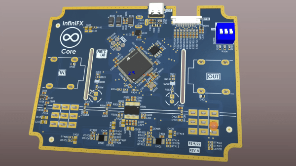
PCB-Filled Dream Desk Will Only Get Cooler With Age

We all have one. Maybe you’re sitting at it now, or just wishing you were — that perfect desk. You know the one — a place for everything and everything in its place, ample acreage, specialized storage, and top-notch looks. Oh, and blinkenlights. Can’t forget those.

It took four months of hard work, but [Build XYZ]’s dream desk has been finely fabricated into fruition. There’s a lot to unpack with this build, which you can appreciate after the break, but it all started with a donated up/down desk from Progressive Desk. After building the base and putting it through its body weight-driven paces, [Build XYZ] set about making the perfect top, which, as you can see, highlights an assortment of PCBs by encasing them for eternity in resin.

But don’t let your admiration stop there, because the woodworking is just as much a part of the show. In addition to the functional blinkenlights that notify [BuildXYZ] when it’s time to stop working for the day or just take a break, there’s a working wireless charger hiding among the FR4. We can’t wait to look back on this desk in 20 years or so and we also can’t wait to see how PCBs will change over the next 20 years.

This tightly-produced video is a fascinating look into the process of forever immortalizing things in resin. So much resin, in fact, that [Build XYZ] came up a gallon short during the pour and had to wait an excruciatingly long time before more resin showed up. Seeing as how you totally can’t tell at all in the final build, we have maximum respect for [Build XYZ]’s inclusion of this part in the first place, which serves as a warning to the rest of us.

Continue reading “PCB-Filled Dream Desk Will Only Get Cooler With Age”

Shot of CubeTouch, a six sided cube built out of PCBs with each of the top PCB allowing for diffusion of the LEDs on the inside to shine through

Keyboard Shortcuts At The Touch Of A Planetary Cube

[Noteolvides] creates the CubeTouch, a cube made of six PCBs soldered together that creates a functional and interactive piece of art through its inlaid LEDs and capacitive touch sensors.

The device itself is connected through a USB-C connector that powers the device and allows it to send custom keyboard shortcuts, depending on which face is touched.

Finger touching the top of a CubeTouch device

The CubeTouch is illuminated on the inside with six WS2812 LEDs that take advantage of the diffusion properties of the underlying FR4 material to shine through the PCBs. The central microprocessor is a CH552 that has native USB support and is Arduino compatible. Each “planet” on the the five outward facing sides acts as a capacitive touch sensor that can be programmed to produce a custom key combination.

Assembling the device involves soldering the connections at two joints for each edge connecting the faces.

We’re no strangers to building enclosures from FR4, nor are we strangers to merging art and functionality. The CubeTouch offers a further exploration of these ideas in a sweet package.

The CubeTouch is Open Source Hardware Certified with all documentation, source code and other relevant digital artifacts available under a libre/free license.

Continue reading “Keyboard Shortcuts At The Touch Of A Planetary Cube”

What Every PCB Designer Needs To Know About Track Impedance With Eric Bogatin

PCB design starts off being a relatively easy affair — you create a rectangular outline, assign some component footprints, run some traces, and dump out some Gerber files to send to the fab. Then as you get more experienced and begin trying harder circuits, dipping into switching power supplies, high speed digital and low noise analog, things get progressively more difficult; and we haven’t even talked about RF or microwave design yet, where things can get just plain weird from the uninitiated viewpoint. [Robert Feranec] is no stranger to such matters, and he’s teamed up with one of leading experts (and one of this scribe’s personal electronics heroes) in signal integrity matters, [Prof. Eric Bogatin] for a deep dive into the how and why of controlled impedance design.

RG58 cable construction. These usually are found in 50 Ω and less commonly these days 75Ω variants

One interesting part of the discussion is why is 50 Ω so prevalent? The answer is firstly historical. Back in the 1930s, coaxial cables needed for radio applications, were designed to minimize transmission loss, using reasonable dimensions and polyethylene insulation, the impedance came out at 50 Ω. Secondarily, when designing PCB traces for a reasonable cost fab, there is a trade-off between power consumption and noise immunity.

As a rule of thumb, lowering the impedance increases noise immunity at the cost of more power consumption, and higher impedance goes the other way. You need to balance this with the resulting trace widths, separation and overall routing density you can tolerate.

Another fun story was when Intel were designing a high speed bus for graphical interfaces, and created a simulation of a typical bus structure and parameterized the physical constants, such as the trace line widths, dielectric thickness, via sizes and so on, that were viable with low-cost PCB fab houses. Then, using a Monte Carlo simulation to run 400,000 simulations, they located the sweet spot. Since the via design compatible with the cheap fab design rules resulted often in a via characteristic impedance that came out quite low, it was recommended to reduce the trace impedance from 100 Ω to 85 Ω differential, rather than try tweak the via geometry to bring it up to match the trace. Fun stuff!

We admit, the video is from the start of the year and very long, but for such important basic concepts in high speed digital design, we think it’s well worth your time. We certainly picked up a couple of useful titbits!

Now we’ve got the PCB construction nailed, why circle back and go check those cables?

Continue reading “What Every PCB Designer Needs To Know About Track Impedance With Eric Bogatin”

Circuit-less PCB Featured As Faceplate For A Digital Clock

If there’s no circuitry on a printed circuit board, does it cease being a “PCB” and perhaps instead become just a “PB”?

Call them what you will, the fact that PCBs have become so cheap and easy to design and fabricate lends them to more creative uses than just acting as the wiring for a project. In this case, [Jeremy Cook] put one to work as the faceplate for his “742 Clock,” a name that plays on the fact that his seven-segment display is 42 mm tall, plus it’s “24/7” backward.

In addition to the actual circuit board that holds the Wemos ESP32 module and the LEDs, a circuit-less board was designed with gaps in the solder mask to act as light pipes. Sandwiched between the boards is a 3D printed mask, to control the light and direct it only through the light pipes. [Jeremy] went through a couple of iterations of diffuser and mask designs, finally coming up with a combination that works well and looks good. He mentions a possible redesign of the faceplate board to include a copper backplane for better opacity, which we think is a good idea. We’d also like to see how different substrates work; would boards of different thickness or using FR-4 with different glass transition temperatures work better? Check out the video below and see what you think.

We’re seeing more and more PCBs turn up as structural elements, from enclosures to control panels and even tools, and we approve of this trend. But what we really approve of is what [Jeremy] did here by making this clock just a dumb display that gets network time over NTP. Would that all three digital clocks in our kitchen did the same thing — maybe then they wouldn’t each be an infuriating minute out of sync with the others.

Continue reading “Circuit-less PCB Featured As Faceplate For A Digital Clock”

Art of 3D printer in the middle of printing a Hackaday Jolly Wrencher logo

Forget The UV Resist Mask: Expose Custom PCBs Directly On Your SLA Printer

For the enterprising hobbyist and prototyping hardware developer, creating custom PCBs remains somewhat of a struggle. Although there are a number of approaches to go about this, they usually involve printing or drawing a mask that is used to expose the photoresist layer on the to-be-etched PCB. Here [Andrew Dickinson]’s Photonic Etcher project provides an intriguing shortcut, by using the UV source of an MSLA 3D printer directly after converting the project’s Gerber files into a format the MSLA printer can work with.

The concept is as simple as can be: since MSLA printers essentially function by creating a dynamically updated UV mask (either via an LCD panel or DLP system), this means that an MSLA printer can be used to expose the PCB’s UV-sensitive photoresistive coating, effectively making the mask there insoluble during the etching step. This can be done with negative as well as positive photoresistive coatings, depending on the use case.

The obvious advantage of this approach is that you don’t need an additional UV source or any kind of separate mask, only an MSLA printer with a large enough work area to fit the PCB you wish to expose. One limitation of [Andrew]’s project at this point is that it can only convert Gerbers to PWMS (Photon Mono) files, but this can presumably be fairly easily extended to support more MSLA printers.

Berlin Clock Takes Inspiration From Sci-Fi Sources, Looks Incredible

What would a HAL9000 look like if it eye were yellow and sat atop a front panel inspired by an Altair 8800? You’d have today’s feature, [Stephan]’s BerlinUhr, a gorgeous little take on a Berlin Clock.

At Hackaday, we have a soft spot for clock builds. They’ve graced our pages from early times. When we saw this ultra cool Berlin Clock, we couldn’t resist the urge to share it with all of our readers.  For those of you not familiar with a Berlin Clock, it’s a clock that consists of 24 lights, and was the first of its kind back in 1975.

[Stephan]’s build is notable because not only is it a beautiful design, but the work that went into the design and build. At several inches tall, the BerlinUhr is supported solely by a USB-C connection, although it can also be hung on a wall. The RTC is backed up by a CR1216, and an ATtiny167 provides the brains for the operation.

A neat part of the build comes with the KPS-3227 light sensor, used to adjust the LED brightness according to ambient lighting. Rather than being a straightforward part to insert into the PCB, KiCad’s footprint had some pins reversed, causing [Stephan] to learn how to correct it and contribute the fix to KiCad. Well done!

We weren’t kidding about clocks, by the way- check out the link to the Atomic Wrist Watch on this post from 2005, and this Russian VFD based clock from 2006- with video!

Do you have your own favorite clock build you’d love to see grace our pages? Be sure to submit a tip!

Panelize PCBs Graphically With Hm-panelizer

When you’re working with PCBs and making single units to knock out in those Chinese fabs, going from layout to manufacturable Gerber files is just a few button presses, no matter what PCB layout tool you prefer. But, once you get into producing sets of PCBs that form a larger system, or are making multiple copies for efficient manufacturing, then you’re not going to get far without delving into the art of PCB panelization. We’ve seen a few options over the years, and here’s yet another one that’s looking quite promising —  hm-panelizer by [halfmarble] is a cross platform Python GUI application, which leverages Kivy, so it should run on pretty well on most major platforms without too much hassle. The tool is early in development, so is restricted to handling only straight PCB edges, with horizontal mouse-bites for now, but we’re sure it will quickly grow more general purpose capabilities given time and support.

In an ideal world, open source tools like KiCAD would have a built-in panelizer, but for now we can dream and hm-panelizer might just be good enough for some people. For more choices on panelizing, checkout our guide to making it easy, and just to muddy the waters here’s another way to do it.