Snapping pictures is not technically difficult with modern technology, but taking good photographs is another matter. There are a number of things that a photographer needs to account for in order to get the best possible results, and if the subject matter isn’t particularly photogenic to start with it makes the task just a little more difficult. As anyone who’s posted something for sale online can attest, taking pictures of everyday objects can present its own challenges even to seasoned photographers. [Martijn Braam] has a few tricks up his sleeve for pictures like this in his efforts to photograph various circuit boards.
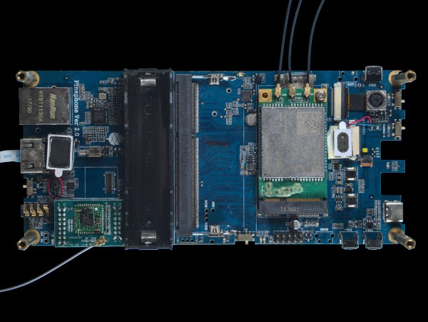
[Martijn] has been updating the images on Hackerboards, an online image reference for single-board computers and other PCBs, and he demands quality in his uploads. To get good pictures of the PCBs, he starts with ample lighting in the form of two wirelessly-controlled flashes in softboxes. He’s also using a high quality macro lens with low distortion, but the real work goes into making sure the image is sharp and the PCBs have well-defined edges. He’s using a Python script to take two pictures with his camera, and some automation in ImageMagic to composite the two images together.
While we’re not all taking pictures of PCBs, it’s a great way of demonstrating the ways that a workflow can be automated in surprising ways, not to mention the proper ways of lighting a photography subject. There are some other excellent ways of lighting subjects that we’ve seen, too, including using broken LCD monitors, or you can take some of these principles to your workspace with this arch lighting system.