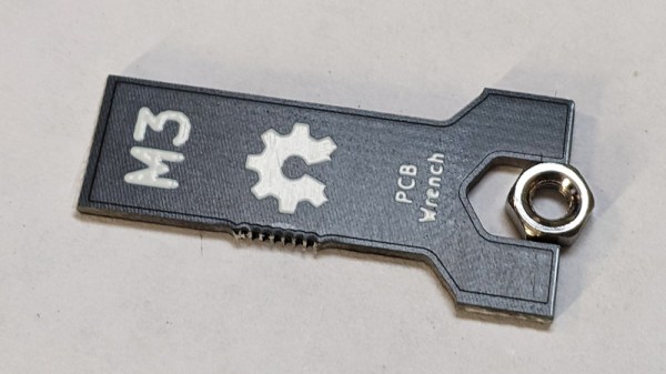
Let’s make one thing abundantly clear. We do not, under any circumstances, recommend you replace your existing collection of wrenches with ones made out of PCBs. However, as creator [Ben Nyx] explains, they do make for an extremely cheap and lightweight temporary tool that would be perfect for distributing with DIY kits.
 This clever open hardware project was spawned by [Ben]’s desire to pack an M3 wrench in with the kits for an ESP32-based kiln controller he’s developing. He was able to find dirt cheap screwdrivers from the usual import sites, but nobody seemed to stock a similarly affordable wrench. He experimented with 3D printing them, but in the end, found the plastic just wasn’t up to the task. Then he wondered how well a tiny wrench cut from a PCB would fare.
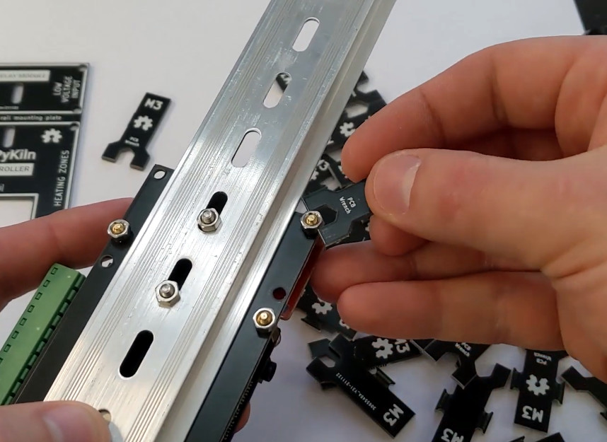
The answer, somewhat surprisingly, is pretty well. We wouldn’t advise you try to crank your lug nuts down with one, but for snugging up a couple nuts that hold down a control board, they work a treat. [Ben] came up with a panelized design in KiCad that allows 18 of the little wrenches to get packed into a 100 x 100 mm PCB suitable for production from popular online board houses. Manufactured from standard 1.6 mm FR4, they come out to approximately 10 cents a pop.
Since [Ben] has been kind enough to release his design under the MIT license, you’re free to spin up some of these wrenches either for your own kits or just to toss in the tool bag for emergencies. We’d love to see somebody adapt the design for additional sizes of nuts, or maybe figure out some way to nest them to sneak out a couple extra wrenches per board.
We’ve seen plenty of folks make cheap tools for themselves in the past, but projects that can produce cheap tools in mass quantities is uniquely exciting for a community like ours.
Continue reading “Ultra Cheap PCB Wrenches Make Perfect Kit Accessory”