If there’s no circuitry on a printed circuit board, does it cease being a “PCB” and perhaps instead become just a “PB”?
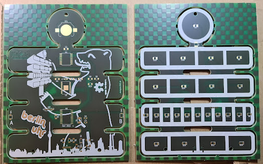
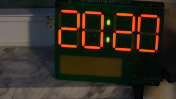
Call them what you will, the fact that PCBs have become so cheap and easy to design and fabricate lends them to more creative uses than just acting as the wiring for a project. In this case, [Jeremy Cook] put one to work as the faceplate for his “742 Clock,” a name that plays on the fact that his seven-segment display is 42 mm tall, plus it’s “24/7” backward.
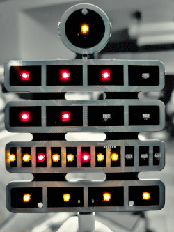
In addition to the actual circuit board that holds the Wemos ESP32 module and the LEDs, a circuit-less board was designed with gaps in the solder mask to act as light pipes. Sandwiched between the boards is a 3D printed mask, to control the light and direct it only through the light pipes. [Jeremy] went through a couple of iterations of diffuser and mask designs, finally coming up with a combination that works well and looks good. He mentions a possible redesign of the faceplate board to include a copper backplane for better opacity, which we think is a good idea. We’d also like to see how different substrates work; would boards of different thickness or using FR-4 with different glass transition temperatures work better? Check out the video below and see what you think.
We’re seeing more and more PCBs turn up as structural elements, from enclosures to control panels and even tools, and we approve of this trend. But what we really approve of is what [Jeremy] did here by making this clock just a dumb display that gets network time over NTP. Would that all three digital clocks in our kitchen did the same thing — maybe then they wouldn’t each be an infuriating minute out of sync with the others.
Continue reading “Circuit-less PCB Featured As Faceplate For A Digital Clock”