Designing circuit boards for high speed applications requires special considerations. This you already know, but what exactly do you need to do differently from common board layout? Building on where I left off discussing impedance in 2 layer Printed Circuit Board (PCB) designs, I wanted to start talking about high speed design techniques as they relate to PCBs. This is the world of multi-layer PCBs and where the impedance of both the Power Delivery Network (PDN) and the integrity of the signals themselves (Signal Integrity or SI) become very important factors.
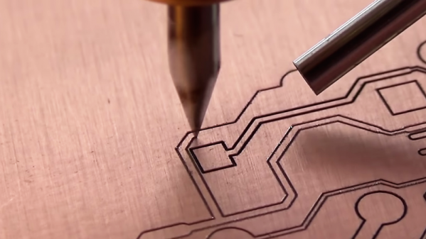
I put together a few board designs to test out different situations that affect high speed signals. You’ve likely heard of vias and traces laid out at right angles having an impact. But have you considered how the glass fabric weave in the board itself impacts a design? In this video I grabbed some of my fanciest test equipment and put these design assumptions to the test. Have a look and then join me after the break for more details on what went into this!
Continue reading “Video: Putting High Speed PCB Design To The Test”