While we typically encourage hackers to make their own tools or machines when practical, x-ray machines don’t usually make that list. Despite the risk of radiation, [William Osman] has done just that and built a homemade x-ray machine. After receiving an eye-watering medical bill, [William] resolves to make his own x-ray machine in the hopes of avoiding future bills. Thanks to his insurance, the total owed was smaller but still ridiculous to those who live in single-payer health care countries, but it got William thinking. What if he could make an x-ray machine to do cheap x-rays?
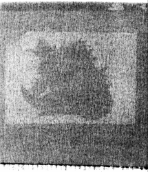
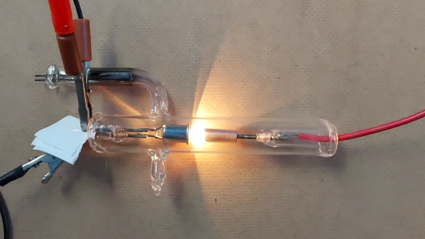
Armed with a cheap high voltage DC power supply he acquired from an online auction house, he started to power up his x-ray vacuum tube. A smaller power supply energizes the cathode and forms an electron beam. Then the high voltage (30-150kv) is applied as a tube voltage, accelerating the electrons into x-rays. Safety measures are taken somewhat haphazardly with Geiger counters and lead sheets. With a finger bone cast in ballistic shell [William] made his first x-ray with a long exposure on a DSLR. The next items to go in the x-ray “chamber” were a phone and a hand. The results were actually pretty decent and you can clearly see the bones.
We’ve seen homemade X-Ray machines here at Hackaday before, but not one that is constructed perhaps so haphazardly — his approach makes this obvious: don’t try this at home. Video after the break.
We’ll just go ahead and say it right up front: we love teardowns. Ripping into old gear and seeing how engineers solved problems — or didn’t — is endlessly fascinating, even for everyday devices like printers and radios. But where teardowns really get interesting is when the target is something so odd and so specialized that you wouldn’t normally expect to get a peek at the outside, let alone tramp through its guts.
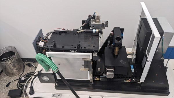
[Mads Barnkob] happened upon one such item, a Fujifilm FCR XG-1 digital radiography scanner. The once expensive and still very heavy piece of medical equipment was sort of a “digital film system” that a practitioner could use to replace the old-fashioned silver-based films used in radiography, without going all-in on a completely new digital X-ray suite. It’s a complex piece of equipment, the engineering of which yields a lot of extremely interesting details.
The video below is the third part of [Mads]’ series, where he zeroes in on the object of his desire: the machine’s photomultiplier tube. The stuff that surrounds the tube, though, is the real star, at least to us; that bent acrylic light pipe alone is worth the price of admission. Previous videos focused on the laser scanner unit inside the machine, as well as the mechatronics needed to transport the imaging plates and scan them. The video below also shows experiments with the PM tube, which when coupled with a block of scintillating plastic worked as a great radiation detector.
Can I just say that doing a links roundup article in a week that includes April Fool’s Day isn’t a fun job? Because it’s not. I mean, how can you take something like reports of X-rays flowing from Uranus seriously when they release the report on such a day? It sure looks like a legitimate story, though, and a pretty interesting one. Planets emitting X-rays isn’t really a new thing; we’ve known that Jupiter and Saturn are both powerful X-ray sources for decades. Even though Uranus is the odd child of our solar system, finding evidence for X-ray emissions buried in data captured by the Chandra observatory in 2007 was unexpected. Astronomers think the X-rays might be coming from Uranus’ rings, or they might be reflections of X-rays streaming out from the sun. Or, it might be the weird alignment of the gas giant’s magnetic field causing powerful aurorae that glow in the X-ray part of the spectrum. Whatever it is, it’s weird and beautiful, which all things considered isn’t a bad way for things to be.
Another potential jest-based story popped up this week about the seemingly impossible “EmDrive”. It seems that when you appear to be breaking the laws of physics, you’re probably doing it wrong, and careful lab tests showed that fuel-free propulsion isn’t here yet. One would think it was self-obvious that filling a closed asymmetrical chamber with microwaves would produce absolutely no thrust, but EmDrive proponents have reported small but measurable amounts of thrust from the improbable engine for years. A team at TU Dresden found otherwise, though. Even though they were able to measure a displacement of the engine, it appears to be from the test stand heating up and warping as the RF energy flowed into the drive chamber. By changing the way the engine was supported, they were able to cancel out the dimensional changes that were making it look like the EmDrive was actually working.
Want to use surface-mount parts, but don’t want to bother spinning up an SMD board? Not a problem, at least if you follow the lead of David Buchanan and perform no-surface surface-mount prototyping. We stumbled upon this on Twitter and thought it looked cool — it’s got a little bit of a circuit sculpture feeling, and we like the old-school look of plain 0.1″ perfboard. David reports that the flying leads are just enameled magnet wire; having done our share of scraping and cleaning magnet wire prior to soldering, we figured that part of the build must have been painful. We pinged David and asked if he had any shortcuts for prepping magnet wire, but alas, he says he just used a hot blob of solder and a little patience while the enamel cooked off. We still really like the style of this build, and we applaud the effort.
Speaking of stumbling across things, that’s one of the great joys of this job — falling down algorithmically generated rabbit holes as we troll about for the freshest hacks. One such serendipitous was this YouTube channel documenting a really nice jet engine build. We’ve seen plenty of jet engines before, but very few with afterburners like this one has. There’s also something deeply satisfying about the variable-throat nozzle that Praendy built for the engine — it’s a level of complexity that you don’t often see in hobbyist jet engines, and yet the mechanism is very simple and understandable.
The other rabbit hole we discovered was after reporting on this cool TIG tungsten grinding tool. That took us into The Metalist’s back catalog, where we found a lot of interesting stuff. But the real treat was this automatic tube polisher (video), which we have to say kept us guessing up to the very end. If you’ve got 12 minutes and you enjoy metalworking builds at all, watch it and see if you’re not surprised by the cleverness of this tool.
And finally, we had heard of the travails of Anatoli Bugorski before, but never in the detail presented in this disturbing video. (Embedded below.)
Who is Anatoli Bugorski, you ask? He is a Russian particle physicist who, while working in an accelerator lab in 1978, managed to get his head directly in the path of a 76 GeV proton beam. Despite getting a huge dose of radiation, Bugorski not only survived the accident but managed to finish his Ph.D. and went on to a long career in nuclear physics. He also got married and had a son. He was certainly injured — facial paralysis and partial deafness, mainly — but did not suffer anything like the gruesome fates of the Chernobyl firefighters or others receiving massive radiation doses. The video goes into some detail about how the accident happened — two light bulbs are better than one, it turns out. We enjoyed the video, but couldn’t stop thinking that Bugorski was the Russian atomic-age equivalent of Phineas Gage.
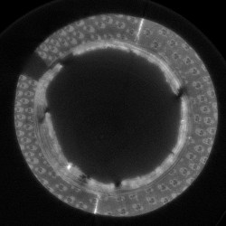
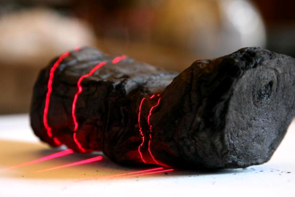
Over recent years we’ve been treated to a series of fascinating advances in the world of x-ray imaging, as researchers have developed their x-ray microtomography techniques and equipment to the point at which they can probe and then computationally reconstruct written material within objects such as letters or scrolls in museum collections whose value or fragility means they can’t be opened and read conventionally. There is more to this challenge than simply extracting the writing though, in addition to detecting the ink the researchers also have to unpick the structure of whatever it was written upon. A particular challenge comes from letterpackets, the art of folding a letter into its own envelope, and a newly-published Nature Communications paper details work from a team of academics in the USA, the UK, and the Netherlands in tackling it.
Letterpackets were more than a practical method of packaging a missive for the mail, they also had a security function often called Letterlocking. A packet would be folded in such a way as to ensure it was impossible to open without tearing or otherwise damaging the paper, and their structure is of especial interest to historians. The researchers had a unique resource with which to work; the Brienne collection is a trunk full of undeliverable mail amassed by a 17th century postmaster couple in Den Haag in the Netherlands, and now in the possession of the Beeld en Geluid museum in that city. In it were a cache of letters including 577 never-opened letterpackets, and the x-ray technique promised a means to analyse these without compromising them.
The researchers have developed an entirely computational technique for the virtual unfolding process. Starting with a 3D volumetric x-ray scan of the unopened packet they then identify the various layers of paper and the bright spots which denote the ink. Their algorithm has to cope with areas in which two or more layers are tightly in contact, for example when multiple levels are folded, and then unpick the resulting 3-dimensional mesh into a 2-dimensional sheet. Their process for mapping the crease pattern involves applying a colour map representing the mean curve radius at a given point. The final section of the paper looks at the multiple different methods of letterlocking, and attempts to categorise them all including a security rating for each. It’s evident that this could be a highly personalised process, indeed they give as an example a letter from Mary Queen of Scots that used an intricate spiral folding technique to identify its sender.
It’s clear that this technique will reveal many more fascinating historical documents as it is both refined and extended across the many more collections of further artefacts that have lain waiting for it. As they say, individual letters do not necessarily contain earth-shattering historical discoveries, but taken together they shed an important light on the social history of past centuries.
When you buy a chip, how can you be sure you’re getting what you paid for? After all, it’s just a black fleck of plastic with some leads sticking out of it, and a few laser-etched markings on it that attest to what lies within. All of that’s straightforward to fake, of course, and it’s pretty easy to tell if you’ve got a defective chip once you try it out in a circuit.
But what about off-brand chips? Those chips might be functionally similar, but still off-spec in some critical way. That was the case for [Kevin Darrah] which led to his forensic analysis of potentially counterfeit MCU chips. [Kevin] noticed that one of his ATMega328 projects was consuming way too much power in deep sleep mode — about two orders of magnitude too much. The first video below shows his initial investigation and characterization of the problem, including removal of the questionable chip from the dev board it was on and putting it onto a breakout board that should draw less than a microamp in deep sleep. Showing that it drew 100 μA instead sealed the deal — something was up with the chip.
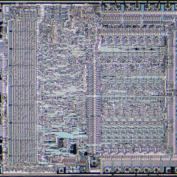
[Kevin] then sent the potentially bogus chip off to a lab for a full forensic analysis, because of course there are companies that do this for a living. The second video below shows the external inspection, which revealed nothing conclusive, followed by an X-ray analysis. That revealed enough weirdness to warrant destructive testing, which showed the sorry truth — the die in the suspect unit was vastly different from the Atmel chip’s die.
It’s hard to say that this chip is a counterfeit; after all, Atmel may have some sort of contract with another foundry to produce MCUs. But it’s clearly an issue to keep in mind when buying bargain-basement chips, especially ones that test functionally almost-sorta in-spec. Caveat emptor.
Counterfeit parts are depressingly common, and are a subject we’ve touched on many times before. If you’d like to know more, start with a guide.
In graduate school, I had a seminar course where one of the sections was about X-ray crystallography. I was excited, because being able to discern the three-dimensional structure of macromolecules just by shining X-rays on them seemed like magic to me. And thanks to a lackluster professor, after the section it remained just as much of a mystery.
If only I’d had [Steve Mould] as a teacher back then. His latest video does an outstanding job explaining X-ray crystallography by scaling up the problem considerably, using the longer wavelength of light and a macroscopic target. He begins with a review of diffraction patterns, those alternating light and dark bands of constructive and destructive interference that result when light shines on two closely spaced slits — the famous “Double-Slit Experiment” that showed light behaves both as a particle and as a wave and provided our first glimpse of quantum mechanics. [Steve] then doubled down on the double-slit, placing another pair of slits in the path of the first. This revealed a grid of spots rather than alternating bands, with the angle between axes dependent on the angle of the slit pairs to each other.
Photograph 51, an X-ray crystallogram of the B-form of DNA, by Gosling and Franklin, 1952. Source: Wikipedia
To complete the demonstration, [Steve] then used diffraction to image the helical tungsten filament of an incandescent light bulb. Shining a laser through the helix resulted in a pattern bearing a striking resemblance to what’s probably the most famous X-ray crystallogram ever: [Rosalind Franklin]’s portrait of DNA. It all makes perfect sense, and it’s easy to see how the process works when scaled down both in terms of the target size and the wavelength of light used to probe it.
Hats off to [Steve] for making something that’s ordinarily complex so easily understandable, and for filling in a long-standing gap in my knowledge.
At risk of getting any ASMR buffs who might be reading cranky because there’s no audio, [Chris], or [@no1089] on Twitter, has gifted us with this visually stunning scan of his Maxim MAX86160 in-ear heart monitor mounted on a rigidflex PCB. You can take a look, in the video below the break.
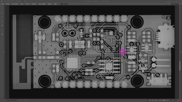
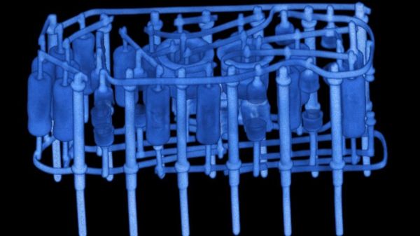
If you’re wondering why anyone would scan a board, other than boredom, know that it’s actually quite common. X-Ray machines are commonly used as a quick, passive way to check a board that’s fresh off the production line. These aren’t the X-Rays like those of broken bones you’re (hopefully not too) used to seeing though, they’re Computed Tomography scans (CT scans, CAT scans), in effect just 3D X-Rays.
For electronics manufacturers and assemblers, CT scans are incredibly useful because they provide a non-destructive way to check for errors. For example, how do you know if that middle BGA pin is actually soldered correctly? You could run a functional test and make sure everything is working (at least, everything you check), but that takes time. The longer it takes to validate, the higher the manufacturing cost. In manager speak: “cost bad. Fast good.”
It’s also common to use a CT scan to create a full 3D model of a board. This makes it easy to check every little detail, especially the ones that are visually obscured by surface mount devices or critical signal paths that are buried under board layers.
But we know you really want more of this video, but better. And we’ve got the goods. For the chill folk among you, here’s a 55-minute version without all the CT scan info cluttering the screen. For those of you currently blasting eDM in your headphones, here’s a 30 second clip of it looping at ~5x speed. Eat your heart out: