Learn Digital Logic By Alien Abduction

Some of the best educational material we’ve seen tells a story. There’s something more fun about reading a story than just absorbing a bunch of dry facts. That’s the idea behind Adventures in Logic Land. In the first episode, you are abducted by aliens trying to decide if humans are intelligent. To prove that, you have to work a series of logic puzzles.

The approach is a little unorthodox. You are shown a live logic simulation (spoiler: it is a NOR gate) and you have to fill in a truth table. The gates use alien symbols which contributes to the storyline but perhaps isn’t the best choice from an educational perspective. Besides, they already use red for zero and green for one which seems a little culturally-specific. The next test shows you how to build your own little simulations and run tests to see if they meet the alien’s criteria.

Continue reading “Learn Digital Logic By Alien Abduction”

Behind The Pin: Logic Level Outputs

There is one thing that unites almost every computer and logic circuit commonly used in the hardware hacking and experimentation arena. No matter what its age, speed, or internal configuration, electronics speak to the world through logic level I/O. A single conductor which is switched between voltage levels to denote a logic 1 or logic zero. This is an interface standard that has survived the decades from the earliest integrated circuit logic output of the 1960s to the latest microcontroller GPIO in 2018.

The effect of this tried and true arrangement is that we can take a 7400 series I/O port on an 8-bit microcomputer from the 1970s and know with absolute confidence that it will interface without too much drama to a modern single-board computer GPIO. When you think about it, this is rather amazing.

It’s tempting to think then that all logic level outputs are the same, right? And of course they are from a certain viewpoint. Sure, you may need to account for level shifting between for example 5V and 3.3V families but otherwise just plug, and go, right? Of course, the real answer isn’t quite that simple. There are subtle electrical differences between the properties of I/O lines of different logic and microcontroller families. In most cases these will never be a problem at all, but can rear their heads as edge cases which the would-be experimenter needs to know something about.

Continue reading “Behind The Pin: Logic Level Outputs”

Online Logic Simulator Is Textual — No, Graphical

We have a bit of a love/hate relationship with tools in the web browser. For education or just a quick experiment, we love having circuit analysis and FPGA tools at our fingertips with no installation required. However, we get nervous about storing code or schematics we might like to keep private “in the cloud.” However, looking at [Lode Vandevenne’s] LogicEmu, we think it is squarely in the educational camp.

You can think of this as sort of Falstad for logic circuits (although don’t forget Falstad does logic, too). The interface is sort of graphical, and sort of text-based, too. When you open the site, you’ll see a welcome document. But it isn’t just a document, it has embedded logic circuits in it that work.

Continue reading “Online Logic Simulator Is Textual — No, Graphical”

FPGA Clocks For Software Developers (or Anyone)

It used to be that designing hardware required schematics and designing software required code. Sure, a lot of people could jump back and forth, but it was clearly a different discipline. Today, a lot of substantial digital design occurs using a hardware description language (HDL) like Verilog or VHDL. These look like software, but as we’ve pointed out many times, it isn’t really the same. [Zipcpu] has a really clear blog post that explains how it is different and why.

[Zipcpu] notes something we’ve seen all too often on the web. Some neophytes will write sequential code using Verilog or VHDL as if it was a conventional programming language. Code like that may even simulate. However, the resulting hardware will — at best — be very inefficient and at worst will not even work.

Continue reading “FPGA Clocks For Software Developers (or Anyone)”

Cheap Powerbank Logic And Teardown

A fixture on many British high streets are pound shops. You may have an equivalent wherever in the world you are reading this; shops in which everything on sale has the same low price. They may be called dollar stores, one-Euro stores, or similar. In this case a pound, wich translates today to a shade under $1.24.

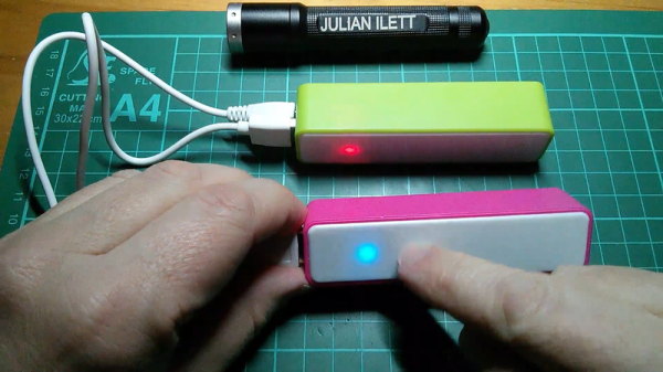
Amid the slightly random selection of groceries and household products are a small range of electronic goods. FM radios, USB cables and hubs, headphones, and mobile phone accessories. It was one of these that caught [Julian Ilett]’s eye, a USB power bank. (Video embedded below.)

You don’t get much for a quid, and it shows in this product. A USB cable that gets warm at the slightest current, a claimed 800 mA of output at 5V from a claimed 1200 mAh capacity, and all from an 18650 Li-ion cell of indeterminate origin. The active component is an FM9833E SOIC-8 switching regulator and charger (220K PDF data sheet, in Chinese).

A straightforward teardown of a piece of near-junk consumer electronics would not normally be seen as something we’d tempt you with, but [Julian] goes on to have some rather pointless but entertaining fun with these devices. If you daisy-chain them, they can be shown to have the properties of rudimentary digital logic, and in the video we’ve put below the break it is this that he proceeds to demonstrate. We see a bistable latch, a set-reset latch, a very slow astable multivibrator, and finally he pulls out a load more power banks for a ring oscillator.

If only [MacGyver] had found himself trapped in a container of power banks somewhere from which only solving a complex mathematical conundrum could release him, perhaps he could have fashioned an entire computer! The best conclusion is the one given at the end of the video by [Julian] himself, in which he suggests (and we’re paraphrasing here) that if you feel the idea to be unworthy of merit, you can tell him so in the comments.

Continue reading “Cheap Powerbank Logic And Teardown”

DIY Computer — 1968 Style

What does it mean to “build your own computer?” Today, it is likely to mean you bought a motherboard, a power supply, and a case and put it all together. You might even have made an embedded computer using a few chips, including an off the shelf CPU. However, there are those guys (like me) who have built entire computers using FPGAs and some (not like me) who have built computers out of TTL chips, discrete components, and even relays and we have covered quite a few of them.

It hasn’t always been that easy. Components are readily available now and relatively cheap (especially considering inflation). In the 1960’s, simple components cost more than you pay for them today and back then your hypothetical self was making less money. In just about every way imaginable, the cost was prohibitive.

clipSo what did you do if you were a kid saving money from a paper route in 1968 and you wanted to build a computer? Maybe you turned to How to Build a Working Digital Computer a book published in 1968 by [Edward Alcosser], [James Phillips], and [Allen Wolk]. This book did as the title promised: you could build a working digital computer. The components, though, were paper clips, tin cans, thread spools, and other household items. The only real electronic components you had to use were light bulbs and a battery, although you might also use store-bought switches in some places instead of the homemade versions shown in the book.

Continue reading “DIY Computer — 1968 Style”

Learn Flip Flops With (More) Simulation

In the previous installment, we talked about why flip flops are such an important part of digital design. We also looked at some latch circuits. This time, I want to look at some actual flip flops–that is circuit elements that hold their state based on some clock signal.

Just like last time, I want to look at sequential building blocks in three different ways: at the abstraction level, at the gate level, and then using Verilog and two online tools that you can also use to simulate the circuits. Remember the SR latch? It takes two inputs, one to set the Q output and the other to reset it. This unassuming building block is at the heart of many other logic circuits.

circ5A common enhancement to the SR latch is to include an enable signal. This precludes the output from changing when the enable signal is not asserted. The implementation is simple. You only need to put an additional gate on each input so that the output of the gate can’t assert unless the other input (the enable) is asserted. The schematic appears on the right.

In the case of this simulation (or the Verilog equivalent), the SR inputs become active high because of the inversion in the input NAND gates. If the enable input is low, nothing will change. If it is high, then asserted inputs on the S or R inputs will cause the latch to set or reset. Don’t set both high at the same time when the enable is high (or, go ahead–it is a simulation, so you can’t burn anything up).(Note: If you can’t see the entire circuit or you see nothing in the circuit simulator, try selecting Edit | Centre Circuit from the main menu.)

Continue reading “Learn Flip Flops With (More) Simulation”