Inside Digital Image Chips

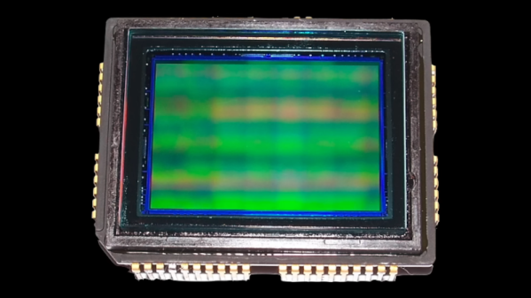
Have you ever thought how amazing it is that every bit of DRAM in your computer requires a teeny tiny capacitor? A 16 GB DRAM has 128 billion little capacitors, one for each bit. However, that’s not the only densely-packed IC you probably use daily. The other one is the image sensor in your camera, which is probably in your phone. The ICs have a tremendous number of tiny silicon photosensors, and [Asianometry] explains how they work in the video you can see below.

The story starts way back in the 1800s when Hertz noticed that light could knock electrons out of their normal orbits. He couldn’t explain exactly what was happening, especially since the light intensity didn’t correlate to the energy of the electrons, only the number of them. It took Einstein to figure out what was going on, and early devices that used the principle were photomultiplier tubes, which are extremely sensitive. However, they were bulky, and an array of even dozens of them would be gigantic.

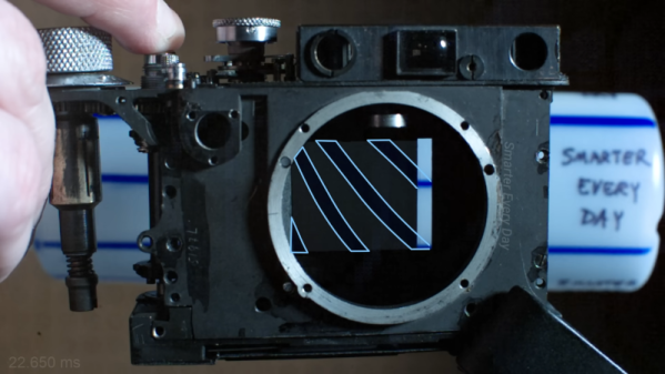
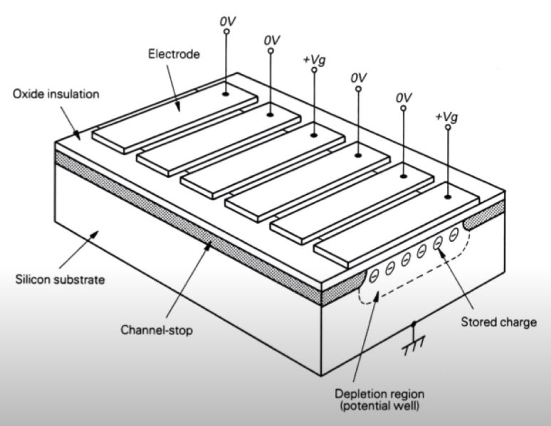
Semiconductor devices use silicon. Bell Labs was working on bubble memory, which was a way of creating memory that was never very popular. However, as a byproduct, the researchers realized that moving charges around for memory could also move around charges from photosensitive diodes. The key idea was that it was harder to connect many photodiodes than it was to create the photodiodes. Using the charge-coupled device or CCD method, the chip could manipulate the charges to reduce the number of connections to the chip.

CCDs opened up the digital image market, but it has some problems. The next stage was CMOS chips. They’d been around for a while since IBM produced the scanistor, but the sensitivity of these CMOS image chips was poor. Since most people were happy with CCD, there wasn’t as much research on CMOS. However, CMOS sensors would eventually become more capable, and the video explains how it works.

We’ve looked at image sensors before, too. The way you read them can make a big difference in your images.

Continue reading “Inside Digital Image Chips”

Dobsonian Telescope Adds Plate Solver

The amateur astronomy world got a tremendous boost during the 1960s when John Dobson invented what is now called the Dobsonian telescope. Made from commonly-sourced materials and mechanically much simpler than what was otherwise available at the time, the telescope dramatically reduced the barrier to entry for larger telescopes and also made them much more portable and inexpensive.

For all their perks, though, a major downside is increased complexity when building automatic tracking systems. [brickbots] went a different way when solving this problem, though: a plate solver.

Plate solving is a method by which the telescope’s field of view is compared to known star charts to determine what it’s currently looking at. Using a Raspberry Pi at the center of the build, the camera module pointed at the sky lets the small computer know exactly what it’s looking at, and the GPS system adds precise location data as well for a quick plate solving solution. A red-tinted screen finishes out the build and lets [brickbots] know exactly what the telescope is pointed towards at all times.

While this doesn’t fully automate or control the telescope like a tracking system would do, it’s much simpler to build a plate solver in this situation. That doesn’t mean it’s impossible to star hop with a telescope like this, though; alt-azimuth mounted telescopes like Dobsonians just need some extra equipment to get this job done. Here’s an example which controls a similar alt-azimuth telescope using an ESP32 and a few rotary encoders.

AI And Savvy Marketing Create Dubious Moon Photos

Taking a high-resolution photo of the moon is a surprisingly difficult task. Not only is a long enough lens required, but the camera typically needs to be mounted on a tracking system of some kind, as the moon moves too fast for the long exposure times needed. That’s why plenty were skeptical of Samsung’s claims that their latest smart phone cameras could actually photograph this celestial body with any degree of detail. It turns out that this skepticism might be warranted.

Samsung’s marketing department is claiming that this phone is using artificial intelligence to improve photos, which should quickly raise a red flag for anyone technically minded. [ibreakphotos] wanted to put this to the test rather than speculate, so a high-resolution image of the moon was modified in such a way that most of the fine detail of the image was lost. Displaying this image on a monitor, standing across the room, and using the smartphone in question reveals details in the image that can’t possibly be there.

The image that accompanies this post shows the two images side-by-side for those skeptical of these claims, but from what we can tell it looks like this is essentially an AI system copy-pasting the moon into images it thinks are of the moon itself. The AI also seems to need something more moon-like than a ping pong ball to trigger the detail overlay too, as other tests appear to debunk a more simplified overlay theory. It seems like using this system, though, is doing about the same thing that this AI camera does to take pictures of various common objects.

Measuring A Millisecond Mechanically

If you are manufacturing something, you have to test it. It wouldn’t do, for example, for your car to say it was going 60 MPH when it was really going 90 MPH. But if you were making a classic Leica camera back in the early 20th century, how do you measure a shutter that operates at 1/1000 of a second — a millisecond — without modern electronics? The answer is a special stroboscope that would look at home in any cyberpunk novel. [SmarterEveryDay] visited a camera restoration operation in Finland, and you can see the machine in action in the video below.

The machine has a wheel that rotates at a fixed speed. By imaging a pattern through the camera, you can determine the shutter speed. The video shows a high-speed video of the shutter operation which is worth watching, and it also explains exactly how the rotating disk combined with the rotating shutter allows the measurement. Continue reading “Measuring A Millisecond Mechanically”

[Bunnie] Peeks Inside ICs With IR

If you want to see inside an integrated circuit (IC), you generally have to take the die out of the package, which can be technically challenging and often destroys the device. Looking to improve the situation, [Bunnie] has been working on Infra-Red, In Situ (IRIS) inspection of silicon devices. The technique relies on the fact that newer packages expose the backside of the silicon die and that silicon is invisible to IR light. The IR reflects off the bottom metalization layer and you can get a pretty good idea of what’s going on inside the chip, under the right circumstances.

As you might expect, the resolution isn’t what you’d get from, say, a scanning electron microscope or other techniques. However, using IR is reasonably cheap and doesn’t require removal from the PCB. That means you can image exactly the part that is in the device, without removing it. Of course, you need an IR-sensitive camera, which is about any camera these days if you remove the IR filter from it. You also need an IR source which isn’t very hard to do these days, either.

Do you need the capability to peer inside your ICs? You might not. But if you do and you can live with the limitations of this method, it would be a very inexpensive way to get a glimpse behind the curtain.

If you want to try the old-fashioned way, we can help. Just don’t expect to be as good as [Ken] at doing it right away.

Continue reading “[Bunnie] Peeks Inside ICs With IR”

Your Phone Is A 200X Microscope — Sort Of

[A. Cemal Ekin] over on PetaPixel reviewed the Apexel 200X LED Microscope Lens. The relatively inexpensive accessory promises to transform your cell phone camera into a microscope. Of course, lenses that strap over your phone’s camera lens aren’t exactly a new idea, but this one looks a little more substantial than the usual piece of plastic in a spring-loaded clip. Does it work? You should read [Cemal’s] post for the details, but the answer — as you might have expected — is yes and no.

On the yes side, you can get some pretty neat photomicrographs from the adapter. On the negative side, your phone isn’t made to accommodate microscope samples. It also isn’t made to stay stable at 200X.

Continue reading “Your Phone Is A 200X Microscope — Sort Of”

Collection Of Old Films Rescued For Preservation

Periscope Film owners [Doug] and [Nick] just released a mini-documentary about the rescue of a large collection of old 35 and 16 mm celluloid films from the landfill. The video shows the process of the films being collected from the donor and then being sorted and organized in a temporary storage warehouse. There is a dizzying variety of films in this haul, from different countries, in both color and black and white.

We can see in the video that their rented 8 meter (26 foot) cargo truck wasn’t enough to contain the trove, so they dragged along a 1.8 x 3.6 m (6 x 12 ft) double-axle trailer as well. That makes a grand total of 49 cubic meters of space. Our back-of-the-envelope calculations says that filled to the brim, that would be over 30,000 canisters of 600 m (2,000 ft) 35 mm movie reels.

When it comes to preserving these old films, one big problem is physical deterioration of the film stock itself. You will know something is wrong when you get a strong acetic or vinegary odor when opening the can. [Nick] shows some examples where the film has even become solidified, taken on a hexagonal shape. It will take months to just assess and catalog the contents of this collection, with damaged films that are still salvageable jumping to the head of the queue to be digitized.

Film Scanning Artist [Esteban] Performing Color Correction
Films are digitized at 4K resolution using a Lasergraphics ScanStation archival quality film scanning system, and then the restoration fun begins. One issue demonstrated in this video is color deterioration. In the Eastmancolor film technology introduced in the 1950s, the blue dyes deteriorate over time. This, and a plethora of other issues, are corrected in the restoration process.

We’re particularly jealous of film scanning artist [Esteban]’s triple-headed trackball. We learned from a quick Google search this beast is merely the entry level control panel from UK company Tangent — they make even larger flavors.

If you’re interested in doing this with 8 mm home movies, we covered a project way back in 2011 of a DIY home movie scanning project. We also covered one of Periscope Film’s restored training films about NASA soldering techniques from 1958. Kudos to organizations who focus on keeping these types of interesting and historical films from being dumped in the landfill and lost forever.

Continue reading “Collection Of Old Films Rescued For Preservation”