Most hobbyists say that it is easier to build a functional prototype of an electronic device, than to make the enclosure for it. You could say that there are a lot of ready-made enclosures on the market, but they are never exactly what you need. You could also use a 3D printer to build a custom enclosure, but high-end 3D printers are too expensive, and the cheaper ones produce housings which are often not robust enough, and also require a lot of additional treatment.
Another way is to build the enclosure out of FR4, a material which is commonly used in PCB production. Such enclosures are low-cost, with thin walls but yet very strong, nice looking, pleasant to the touch and have excellent thermal and moisture stability. FR4 offers some more possibilities – efficient wiring with no wires inside the housing, integrated UHF or SHF antennas or RFID coils, capacitive switches, electrical shielding, selective semi-transparency, water or air tightness, and even integration of complex mechanical assemblies.
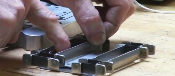
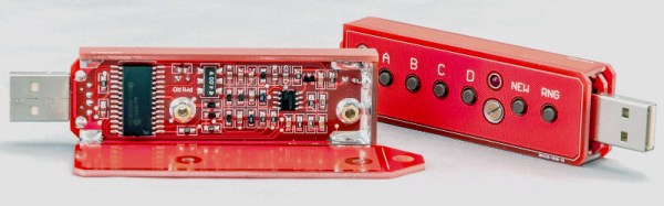
Here I shall explain the process of building those “magic” enclosures. It is based on nearly fifty years of personal experience and more than a hundred enclosures, built for most of my projects. Here are two examples – this case for a hardware password manager is just a few centimeters long, while the other one (protective transportation cover for my son’s synthesizer) measures 125cm (about 49 inches), and yet both of them are strong enough to withstand a grown man standing on top of them.
The global approach is simple – you take the sheet of single-sided copper clad FR4, cut it and solder the parts together. That sounds simple, but there are a lot of details which should be met if you want to get top results. Please read about them carefully. You might be tempted to skip some of the steps described here, but if you do so, you will most likely end up being disappointed with the results.
Continue reading “How To Build Beautiful Enclosures From FR4 — Aka PCBs” →


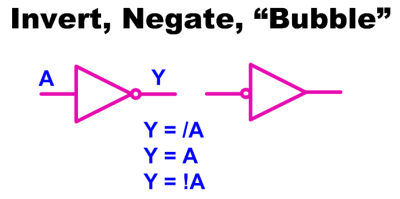 The most simple piece of logic is inversion; making a high change to low or a low change to high. Shown are a couple of ways to write an inversion including the ubiquitous “bubble” that we can apply almost anywhere to imply an inversion or a “True Low”. If it was a one it is now a zero, where it was a low it is now a high, and where it was true it is now untrue.
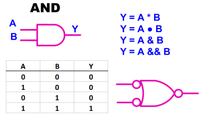 Moving on to the AND gate we see a simple truth table, also known as a Boolean Table, where it describes the function of “A AND B”. This is also our first opportunity to see the application of an alternate symbol. In this case a “low OR a low yields a low”
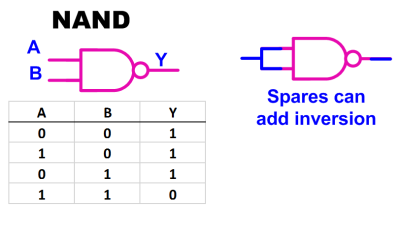 Most if not all of the standard logic blocks come in an inverted form also such as the NAND gate shown here. The ability to invert logic functions is so useful in real life that I probably used at least three times the number of NAND gates as regular AND gates when doing medium or larger system design. The useful inversion can occur as spares or in line with the logic.


