There are at least two ways of making parts that fit together exactly. The first way is the Cartesian way, and the machinists way. Imagine that you could specify the size of both the hole and the peg that you’d like to put into it. Just make sure your tolerances are tight enough, and call out a slightly wider hole. Heck, you can look up the type of fit you’d like in a table, and just specify that. The rest is a simple matter of machining the parts accurately to the right tolerances, and you’re done.
The machinist’s approach lives and dies on that last step — making the parts accurately fit the measure. Contrast the traditional woodworker’s method, or at least as it was taught to me, of just making the parts fit each other in the first place. This is the empirical way, the Aristotelian way if you will. You don’t really have to care if the two parts are exactly 30.000 mm wide, as long as they’re precisely the same length. And woodworkers have all sorts of clever tricks to make things the same, or make them fit, without measuring at all. Their methods are heavy on the jigs and the clever set-ups, and extraordinarily light on the calipers. To me, coming from a “measure carefully, and cut everything to measure” background, these ways of working were a revelation.
This ends up expressing perfectly the distinction between accuracy and precision. Sometimes you need to hit the numbers right on, and other times, you just need to get the parts to fit. And it’s useful to know which of these situations you’re actually in.
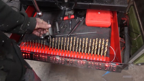
 Of course, none of this is exclusive to metal or wood, and I’m actually mentioning it because I find myself using ideas that I learned in one context and applying them in the other. For instance, if you need sets of holes that match each other perfectly, whether in metal or wood, you get that precision for free by drilling through two sheets at one time, or by making a template — no measuring needed. Instead of measuring an exact distance from a feature, if all you care about is two offsets being the same, you can find a block of scrap with just about the right width, and use that to mark both distances. Is it exactly 1.000″ wide? Nope. But can you use this to mark identical locations? Yup.
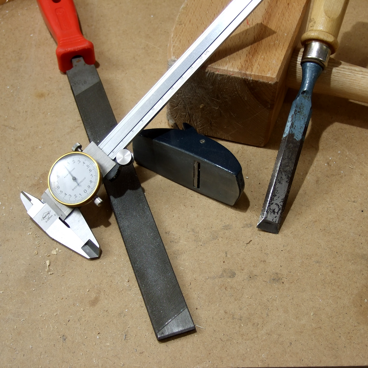
You can make surprisingly round objects in wood by starting with a square, and then precisely marking the centers of the straight faces, and then cutting off the corners to get an octagon. Repeat with the centers and cutting until you can’t see the facets any more. Then hit it with sandpaper and you’re set. While this won’t make as controlled a diameter as would come off a metal lathe, you’d be surprised how well this works for making round sheet-aluminum circles when you don’t care so much about the diameter. And the file is really nothing other than the machinist’s sandpaper (or chisel?).
I’m not advocating one way of working over the other, but recognizing that there are two mindsets, and taking advantage of both. There’s a certain freedom that comes from the machinist’s method: if both parts are exactly 25.4 mm long, they’re both an accurate inch, and they’ll match each other. But if all you care about is precise matching, put them in the vise and cut them at the same time. Why do you bother with the calipers at all? Cut out the middle-man!