A Particularly Festive Chip Decapping

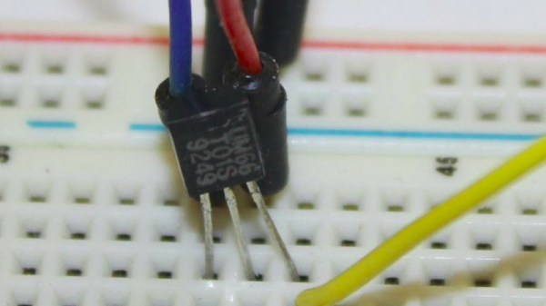
As we approach the moment in the year at which websites enter a festive silly season of scrambling to find any story with a festive angle, we’re pleased to see the ever-reliable [Ken Shirriff] has brought his own take on Christmas tech to the table with a decapping of the UM66T melody chip that has graced so many musical greeting cards.
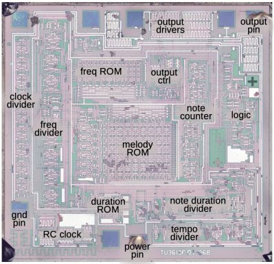
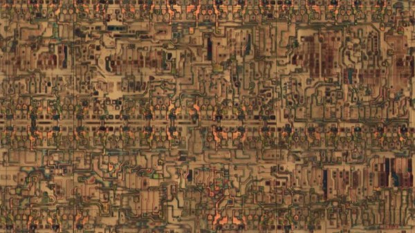
The surprise in this age of ubiquitous microcontrollers is that this is not a smart device; instead it’s a single-purpose logic chip whose purpose is to step through a small ROM containing note values and durations, driving a frequency generator to produce the notes themselves. The frequency generator isn’t the divider chain from the RC oscillator that we might expect, instead it’s a shift register arrangement which saves on the transistor count.

Although the UM66 is a three-pin device, there are a few other pins on the die. These are likely to be for testing. As a 30+ year old product its design may be outdated in 2021, but it’s one of those chips that has survived without being superseded because it does its task without the need for improvement. So when you open a card and hear the tinny tones of a piezo speaker this holiday season, spare a thought for the ingenuity of the design behind the chip that makes it all possible.
Apollo Shift Register Is Discrete

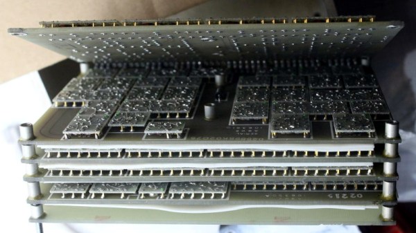
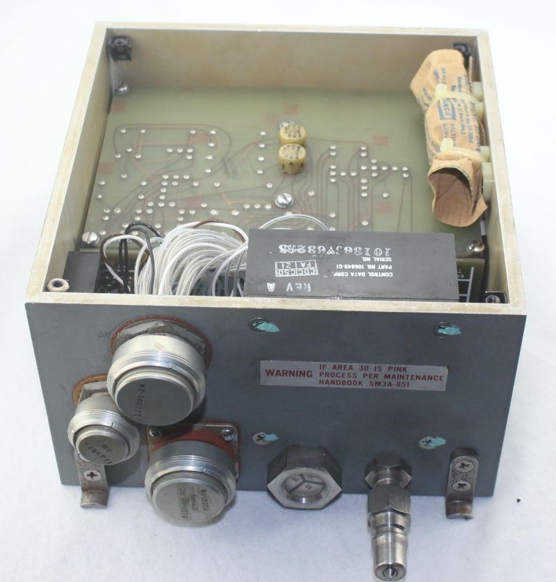
We’re unabashed fans of [Ken Shirriff] here at Hackaday, and his latest post about an Apollo-era transistorized shift register doesn’t disappoint. Of course, nowadays a 16-bit shift register is nothing special. But in 1965, this piece of Apollo test hardware weighed five pounds and likely cost at least one engineer’s salary in the day, if not more.

The incredible complexity of the the Apollo spacecraft required NASA to develop a sophisticated digital system that would allow remote operators to execute tests and examine results from control rooms miles away from the launch pad.

This “Computer Buffer Unit” was used to hold commands for the main computer since a remote operator could not use the DSKY to enter commands directly. Externally the box looks like a piece of military hardware, and on the inside has six circuit boards stacked like the pages of a book. To combat Florida’s notoriously damp conditions, the enclosure included a desiccant bag and a way to fill the device with nitrogen. A humidity indicator warned when it was time to change the bag.

There is a lot more in the post, so if you are interested in unusual construction techniques that were probably the precursor to integrated circuits, diode transistor logic, or just think old space hardware is cool, you’ll enjoy a peek inside this unusual piece of gear. Be sure to check out some of [Ken]’s previous examinations, fromĀ tiny circuits to big computers.

[Ken Shirriff] Picks Apart Mystery Chip From Twitter Photo

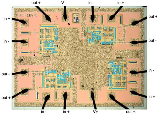
It’s no secret that the work of [Ken Shirriff] graces the front pages of Hackaday quite frequently. He’s back again, this time reverse engineering a comparator chip from a photo on Twitter. The mysterious chip was decapped, photographed under a microscope, and subsequently posted on the internet with an open call to figure out what it did.

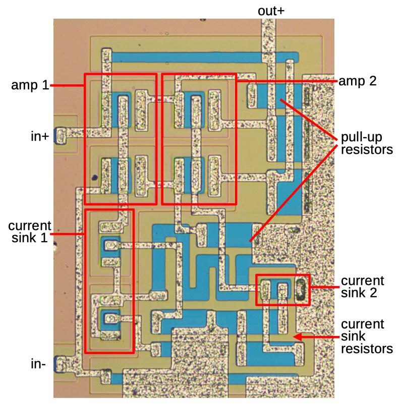
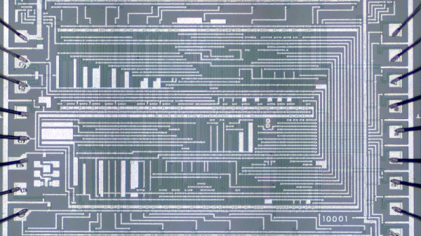
[Ken] stepped up, and at first glance, it was obvious that most of the chip is unused, and there appeared to be four copies of the same circuit. After identifying resistors and the different transistor types, [Ken] found differential pairs.

Differential pairs form the heart of most op-amps, and by chaining them together, you can get a strong enough signal to treat it as a logic signal. Based on the design and materials, [Ken] estimates the chip is from the 1970s. Given that it appears to be ECL (Emitter-Coupled Logic), it could just be four comparators. But there are still a few things that don’t add up as two comparators have additional inverted outputs. Searching the part number offered few if any clues, so this will remain somewhat a mystery.

We’ve covered [Ken’s] incredible chip sleuthing before here, such as the Sharp EL-8 from 1969.

Logic Chip Teardown From Early 1990s IBM ES/9000 Mainframe

The 1980s and early 1990s were a bit of an odd time for semiconductor technology, with the various transistor technologies that had been used over the decades slowly making way for CMOS technology. The 1991-vintage IBM ES/9000 mainframe was one of the last systems to be built around bipolar transistor technology, with [Ken Shirriff] tearing into one of the processor modules (TCM) that made up one of these mainframes.

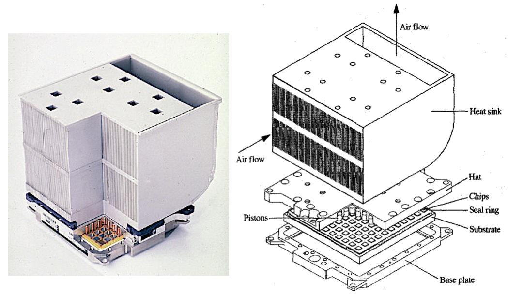
A Thermal Conduction Module from an IBM ES/9000 mainframe.

Five of these Thermal Conduction Modules (127.5 mm a side) made up the processor in these old mainframes. Most of note are the use of the aforementioned bipolar transistors and the use of DCS-based (differential current switch) logic. With the already power-hungry bipolar transistors driven to their limit in the ES/9000, and the use of rather massive DCS gates, each TCM was not only fed many amperes of electricity, but also capable of dissipating up to 600 Watts of power.

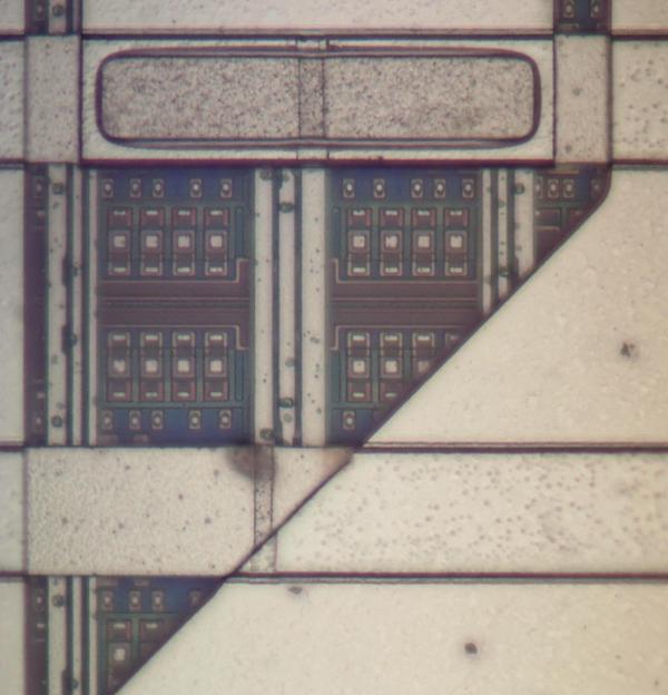
Each TCM didn’t contain a single large die of bipolar transistors either, but instead many smaller dies were bonded on a specially prepared ceramic layer in which the wiring was added through a very precise process. While an absolute marvel of engineering, the ES/9000 was essentially a flop, and by 1997 IBM too would move fully to CMOS transistor technology.

Over the years we’ve featured a lot of [Ken]’s work, perhaps you’d like to know more about his techniques.

Inside An Oscillator With [Ken Shirriff]

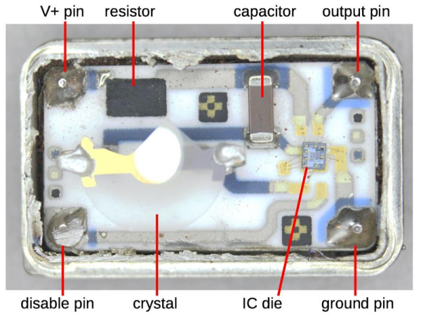
We are always glad to see [Ken Shirriff] tear into something new and this month he’s looking inside a quartz oscillator module. Offhand, you’d think there’s not much to these. A slab of quartz and some sort of inverter, right? But as [Ken] mentions, “There’s more happening in the module than I expected…”

If you’ve ever wanted to decap devices, big hybrid modules like these are a good way to get started since you don’t need exotic chemicals to get at the insides. [Ken] managed to break the fragile crystal wafer on the way in. Inside was also a small CMOS IC die. Time to get out the microscope.

If you follow [Ken’s] blog, you know he’s no stranger to analyzing IC dice. The oscillator IC is a pretty standard Colpitts oscillator but it also provides a programmable divider and output drive.

The circuit uses some unusually configured capacitors. [Ken] takes the time to point out CMOS logic structures throughout. If you haven’t seen one of [Ken’s] deep dives before, before, it’s a great introduction.

You can learn more about crystal oscillator theory. We used some test equipment to characterize a crystal a few years ago.

Reverse Engineering Silicon From The First Pocket Calculator

We’ve seen so many explorations of older semiconductors at the hands of [Ken Shirriff], that we know enough to expect a good read when he releases a new one. His latest doesn’t disappoint, as he delves into the workings of one of the first hand-held electronic calculators. The Sharp EL-8 from 1969 had five MOS ICs at its heart, and among them the NRD2256 keyboard/display chip is getting the [Shirriff] treatment with a decapping and thorough reverse engineering.

The basic functions of the chip are explained more easily than might be expected since this is a relatively simple device by later standards. The fascinating part of the dissection comes in the explanation of the technology, first in introducing the reader to PMOS FETs which required a relatively high negative voltage to operate, and then in explaining its use of four-phase logic. We’re used to static logic that holds a state depending upon its inputs, but the technologies of the day all called for an output transistor that would pull unacceptable current for a calculator. Four phase logic solved this by creating dynamic gates using a four-phase clock signal, relying on the an output capacitor in the gate to hold the value. It’s a technology that lose out in the 1970s as later TTL and CMOS variants arrived that did not have the output current drain. Fascinating stuff!

[Ken] gave a talk at the Hackaday Superconference a couple of years ago, if you’ve not seen it then it’s worth a watch.

What’s Inside An FPGA? Ken Shirriff Has (Again) The Answer

FPGAs are somewhat the IPv6 of integrated circuits — they’ve been around longer than you might think, they let you do awesome things that people are intrigued by initially, but they’ve never really broke out of their niches until rather recently. There’s still a bit of a myth and mystery surrounding them, and as with any technology that has grown vastly in complexity over the years, it’s sometimes best to go back to its very beginning in order to understand it. Well, who’d be better at taking an extra close look at a chip than [Ken Shirriff], so in his latest endeavor, he reverse engineered the very first FPGA known to the world: the Xilinx XC2064.

If you ever wished for a breadboard-friendly FPGA, the XC2064 can scratch that itch, although with its modest 64 configurable logic blocks, there isn’t all that much else it can do — certainly not compared to even the smallest and cheapest of its modern successors. And that’s the beauty of this chip as a reverse engineering target, there’s nothing else than the core essence of an FPGA. After introducing the general concepts of FPGAs, [Ken] (who isn’t known to be too shy to decap a chip in order to look inside) continued in known manner with die pictures in order to map the internal components’ schematics to the actual silicon and to make sense of it all. His ultimate goal: to fully understand and dissect the XC2064’s bitstream.

Of course, reverse engineering FPGA bitstreams isn’t new, and with little doubt, building a toolchain based on its results helped to put Lattice on the map in the maker community (which they didn’t seem to value at first, but still soon enough). We probably won’t see the same happening for Xilinx, but who knows what [Ken]’s up to next, and what others will make of this.