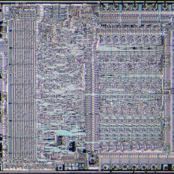
The Flash Memory Lifespan Question: Why QLC May Be NAND Flash’s Swan Song

The late 1990s saw the widespread introduction of solid-state storage based around NAND Flash. Ranging from memory cards for portable devices to storage for desktops and laptops, the data storage future was prophesied to rid us of the shackles of magnetic storage that had held us down until then. As solid-state drives (SSDs) took off in the consumer market, there were those who confidently knew that before long everyone would be using SSDs and hard-disk drives (HDDs) would be relegated to the dust bin of history as the price per gigabyte and general performance of SSDs would just be too competitive.

Fast-forward a number of years, and we are now in a timeline where people are modifying SSDs to have less storage space, just so that their performance and lifespan are less terrible. The reason for this is that by now NAND Flash has hit a number of limits that prevent it from further scaling density-wise, mostly in terms of its feature size. Workarounds include stacking more layers on top of each other (3D NAND) and increasing the number of voltage levels – and thus bits – within an individual cell. Although this has boosted the storage capacity, the transition from single-level cell (SLC) to multi-level (MLC) and today’s TLC and QLC NAND Flash have come at severe penalties, mostly in the form of limited write cycles and much reduced transfer speeds.

So how did we get here, and is there life beyond QLC NAND Flash?

Continue reading “The Flash Memory Lifespan Question: Why QLC May Be NAND Flash’s Swan Song”

Reverse Engineering Reveals EV Charger Has A Sense Of Security

As more and more electric vehicles penetrate the market, there’s going to have to be a proportional rise in the number of charging stations that are built into parking garages, apartment complexes, and even private homes. And the more that happens, the more chargers we’re going to start seeing where security is at best an afterthought in their design.

But as this EV charger teardown and reverse engineering shows, it doesn’t necessarily have to be that way. The charger is a Zaptec Pro station that can do up to 22 kW, and the analysis was done by [Harrison Sand] and [Andreas Claesson]. These are just the kinds of chargers that will likely be widely installed over the next decade, and there’s surprisingly little to them. [Harrison] and [Andreas] found a pair of PCBs, one for the power electronics and one for the control circuits. The latter supports a number of connectivity options, like 4G, WiFi, and Bluetooth, plus some RFID and powerline communications. There are two microcontrollers, a PIC and an ARM Cortex-A7.

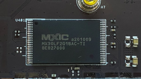
Despite the ARM chip, the board seemed to lack an obvious JTAG port, and while some unpopulated pads did end up having a UART line, there was no shell access possible. An on-board micro SD card slot seemed an obvious target for attack, and some of the Linux images they tried yielded at least a partial boot-up, but without knowing the specific hardware configuration on the board, that’s just shooting in the dark. That’s when the NAND flash chip was popped off the board to dump the firmware, which allowed them to extract the devicetree and build a custom bootloader to finally own root.

The article has a lot of fascinating details on the exploit and what they discovered after getting in, like the fact that even if you had the factory-set Bluetooth PIN, you wouldn’t be able to get free charging. So overall, a pretty good security setup, even if they were able to get in by dumping the firmware. This all reminds us a little of the smart meter reverse engineering our friend [Hash] has been doing, in terms of both methodology and results.

Thanks to [Thinkerer] for the tip.

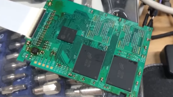
The SSD described, a green board with a ZIP connector, a controller chip and two out of four NAND chips populated. There's traces of flux on the chip, as it hasn't been washed after soldering yet.

ZIF HDDs Dying Out? Here’s An Open-Source 1.8″ SSD

A lot of old technology runs on parts no longer produced – HDDs happen to be one such part, with IDE drives specifically being long out of vogue, and going extinct to natural causes. There’s substitutes, but quite a few of them are either wonky or require expensive storage medium. Now, [dosdude1] has turned his attention to 1.8 ZIF IDE SSDs – FFC-connected hard drives that are particularly rare and therefore expensive to replace, found in laptops like the Macbook Air 1,1 2008 model. Unsatisfied with substitutes, he’s designed an entire SSD from the ground up around an IDE SSD controller and NAND chips. Then, he made the design open-source and filmed an assembly video so that we can build our own. Take a look, we’ve put it below the break!

For an open-source design, there’s a respectable amount of work shared with us. He’s reverse-engineered some IDE SSDs based on the SM2236 controller to design the schematic, and put the full KiCad files on GitHub. In the video, he shows us how to assemble this SSD using only a hot air station and a soldering iron, talks about NAND matching and programming software intricacies, and shows the SSD working in the aforementioned Macbook Air. Certainly, assembly would have been faster and easier with a stencil, but the tools used work great for what’s a self-assembly tutorial!

Continue reading “ZIF HDDs Dying Out? Here’s An Open-Source 1.8″ SSD”

Can You Hot-Swap Flash Chips In A Consumer Router?

Sometimes, you mess up when toying with the firmware of an embedded device and end up “bricking” what you were working on. [Chris Bellows] had done just that with a consumer router, corrupting the onboard NAND flash to the point where recovery via normal means was impossible. Armed with a working duplicate of the router, he wondered if the corrupted NAND flash could be substituted into the working router while it was running, and reflashed in place – and decided to find out.

Key to achieving the hack was finding a way to remove the existing NAND flash in the working router without crashing the system while doing so. This required careful disconnection of the chip’s power lines once the router had booted up, as well as tying the “Ready/Busy” and “Read Enable” pins to ground. With this done, the chip could carefully be removed with a hot air tool without disrupting the router’s operation. The new chip could then be soldered in place, and flashed with factory firmware via the router’s web interface. At this point, it could be powered down and the chips swapped normally back into their own respective routers, restoring both to full functionality.

It’s a neat hack, and one that shows that it’s sometimes worth taking a punt on your crazy ideas just to see what you can pull off. It also pays to know the deeper secrets of the hardware you run on your own home network.

Defeating The Wii Mini As The Internet Watches Over Your Shoulder

Working under the pressure of being watched on a live feed, [DeadlyFoez] pits himself against the so-called unhackable Wii Mini and shows unprecedented results all while recording hours of footage of his process for others to follow along. We dug through that content to find the gems of the process, the links below include timestamps to those moments.

The Wii Mini is a cost-reduced version of Nintendo’s best-selling console, sold near the end of its life with a few features removed such as GameCube backwards compatibility and SD card support. Along with that, in an effort to thwart the jailbreaking that had plagued its big sister Nintendo made it so the NAND memory (where the system is stored) is encrypted and keyed to each device’s Hollywood GPU chip. This defeats methods which modified the storage in order to gain access to the hardware.

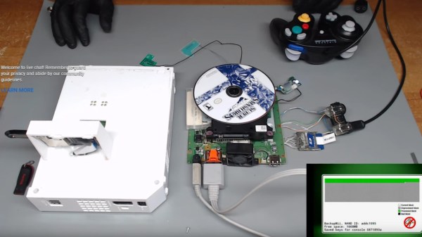
That did not stop [DeadlyFoez] from trying anyway, planning out the steps he needed to achieve a hacked Mini unit with the help of a regular Wii donor, already hacked. After dumping both systems’ NANDs and exploring the Wii Mini hardware further, he found a few pleasant surprises. There are test points on the board which allow GameCube controllers to be used with it. There are also SD card connections physically present on the board, but the support was removed from the Mini’s system software.

The most interesting parts come later on however: by simultaneously swapping NAND and GPU chips between original Wii and Wii Mini, [DeadlyFoez] manages to put together two distinct systems. The first is an original Wii board with the Mini’s chips claimed to be “the first Wii Mini running homebrew software”. The second, filling the opposite side of the equation, with both hardware and software to add SD card and GameCube controller ports to a Wii Mini.

This process of BGA rework in order to mod Nintendo hardware into unorthodox versions of themselves has actually been done before a few years ago, when someone made an unofficial US region non-XL new 3DS by piecing together parts from two separate consoles. Continue reading “Defeating The Wii Mini As The Internet Watches Over Your Shoulder”

Recover Your Broken SD Card Selfies By Your Selfie

You may still have some luck getting those selfies off of your SD card, even if it will no longer mount on your computer. [HDD Recovery Services] shows us a process to directly access the NAND memory of a faulty micro SD card to recover those precious files you thought about backing up but never got around to.

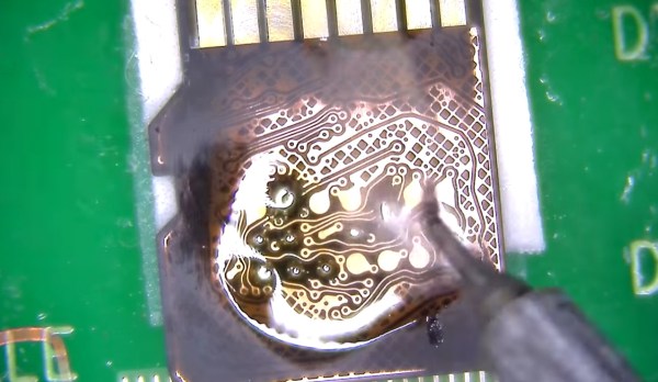
On a Micro SD card you may have noticed there are two slightly longer pins than the rest. These are VSS and VCC pins. As long as they are not a dead short between the two the SD card controller isn’t completely trashed and we can go ahead and get into that little sucker. With a bit of know how — along with sandpaper, enameled wire, and a NAND reader — an image of your lost data can be recovered with a bit of patience and some good soldering skills.

Working your way down from a relatively high grit sand paper, slowly sand away the plastic on the underside of the SD card until you can clearly see the copper traces hidden away inside. Then solder your enameled wire onto the small solder pads to hook it up to a NAND reader and you should be able to read the data that was previously unreachable via conventional means. Of course you’re still going to need to make sense out of the NAND dump. That’s a topic for a different article.

If you ever find yourself in need of an SD card recovery tool you could always roll your own DIY NAND reader. We will likely give this process a try just to play round with the concept. Hopefully we’ll never need to do SD card recovery!

Continue reading “Recover Your Broken SD Card Selfies By Your Selfie”

Arduino Into NAND Reader

[James Tate] is starting up a project to make a “Super Reverse-Engineering Tool”. First on his list? A simple NAND flash reader, for exactly the same reason that Willie Sutton robbed banks: because that’s where the binaries are.

As it stands, [James]’s first version of this tool is probably not what you want to use if you’re dumping a lot of NAND flash modules. His Arduino code reads the NAND using the notoriously slow digital_read() and digital_write() commands and then dumps it over the serial port at 115,200 baud. We’re not sure which is the binding constraint, but neither of these methods are built for speed.

Instead, the code is built for hackability. It’s pretty modular, and if you’ve got a NAND flash that needs other low-level bit twiddling to give up its data, you should be able to get something up and working quickly, start it running, and then go have a coffee for a few days. When you come back, the data will be dumped and you will have only invested a few minutes of human time in the project.

With TSOP breakout boards selling for cheap, all that prevents you from reading out the sweet memory contents of a random device is a few bucks and some patience. If you haven’t ever done so, pull something out of your junk bin and give it a shot! If you’re feeling DIY, or need to read a flash in place, check out this crazy solder-on hack. Or if you can spring for an FTDI FT2233H breakout board, you can read a NAND flash fast using essentially the same techniques as those presented here.