When your widgets have proven so successful that building them gets to be a grind, it might be time to consider a little mechanical help in the form of a pick and place machine (PnP). If you’re going to roll your own though, there’s a lot to think about, not the least of which is how to feed your beast with parts.
Managing the appetite of a PnP is the idea behind this custom modular parts feeder, but the interesting part of [Hans Jørgen Grimstad]’s work-in-progress project has more to do with the design process. The feeders are to support a custom PnP being built in parallel, and so the needs of one dictate the specs of the other. Chief among the specs are the usual big three: cheap, fast, and reliable. But size is an issue too insofar that the PnP could be working with dozens of component reels at once. Flexibility was another design criteria, so that reels of varied width can be accommodated.
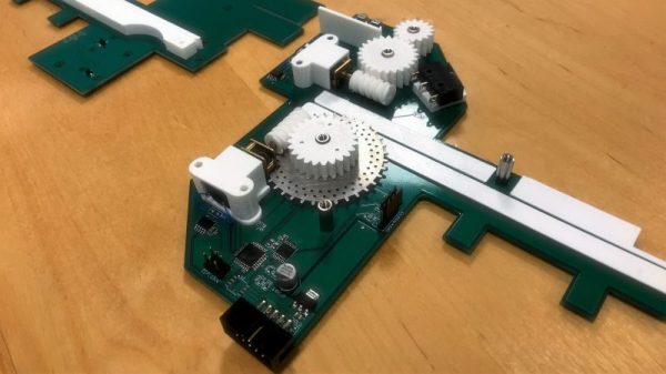
With all that in mind, [Hans] and company came up with a pretty slick design. The frame of the feeder is made out of the PCBs that house the motors for handling the tape, and the ATmega168 that controls everything. Tapes are driven by a laser-cut sprocket driven by 3D-printed worm gears. The boards have fingers that mate up to the aluminum extrusion that the PnP will be built from, and at only a few millimeters wider than the tape, lots of feeders can be nestled together. The video below shows the feeder undergoing some tests.
Alas, this build isn’t quite done, so you’ll have to check back for the final schematics and PCB files if you want to build one for yourself. While you’re waiting, you might want to build your own pick and place.
Continue reading “Custom Parts Feeder Aims To Keep Pace With Pick And Place”