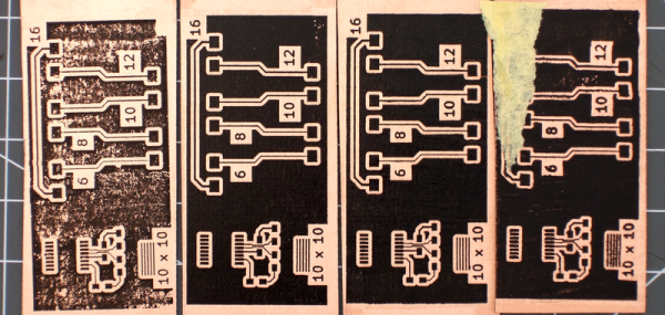
PCB etching seems to be a subject that sharply divides our community into those who are experts in it and etch themselves every PCB they use, and those who have significant quantities of ferric chloride stained clothing in their past and for whom the advent of cheap commercial PCB manufacture and CNC milled PCB prototyping have been the best thing since sliced bread.
Your likely success when etching your own boards is most dependent on the quality of your preparation and your equipment. If you began your PCB career with etch-resist transfers and a permanent marker with a Tupperware tub of etchant, then later progressed to laser toner or photographic masking and a bubble etcher, you’ll understand this.
[Jana Marie Hemsing] has drawn our attention to this very nicely built PCB etching suite (Translation, German original) at the Warpzone hackerspace (Translation, German original) in Münster, Germany. The foil pattern is printed on transparency and exposed to UV light over a photoresist coated board with a vacuum pump arrangement to ensure as good a contact as possible to the board for the sharpest result. They have two exposers, one for single sided and the other for double-sided boards, both are very well-built from what looks like plywood.
The attention to detail continues with a home-made magnetic stirrer and heated bubble etching tank Their etchant of choice is sodium persulphate, so there are none of those brown ferric chloride stains.
PCB etching is nothing new, indeed we have covered the subject extensively over the years. But we think you’ll agree, if you’re going to etch your own PCBs you should have as good a set-up as you can, and Warpzone’s PCB suite is rather well put together. Those of us in spaces with lesser facilities should be getting ideas from it.