Creating New Nintendo 3DS Hardware

For the last five years or so, Nintendo has been selling the 3DS, the latest in a long line of handheld consoles. Around two years ago, Nintendo announced the New Nintendo 3DS, with a faster processor and a few other refinements. The new 3DS comes in two sizes: normal and XL. You can buy the XL version anywhere in the world, but Nintendo fans in North America cannot buy the normal version.

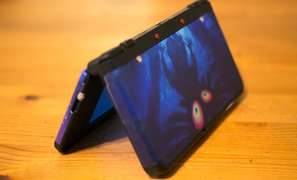
[Stephen] didn’t want the jumbo-sized New 3DS XL, both because it’s too large for his pockets, and because there are no fancy cases for the XL. His solution? Creating a US non-XL 3DS with god-like soldering skills.

In manufacturing the XL and non-XL versions of the 3DS, Nintendo didn’t change much on the PCBs. Sure, the enclosure is different, but electronically there are really only two changes: the eMMC storage and the Nintendo processor. 3DS are region-locked, so simply swapping out the boards from a normal 3DS to an XL 3DS wouldn’t work; [Stephen] would also like to play US games on his modded console. That leaves only one option: desoldering two chips from a US XL and placing them on the board from a Japanese 3DS.

With a board preheater and heat gun, [Stephen] was able to desolder the eMMC chip off both boards. Of course this meant the BGA balls were completely destroyed in the process, which means reballing the package with solder bits only 0.3mm in diameter. With the US eMMC transplanted to the Japanese board, [Stephen] ended up with an error message that suggested the processor was reading the memory. Progress, at least.

[Stephen] then moved on to the processor. This was a nightmare of a 512 pin BGA package, with 512 pins that needed a tiny dot of solder placed on them. Here, sanity gave way and [Stephen] called up a local board and assembly house. They agreed to solder the chip onto the board and do an x-ray inspection. With the professional rework done, [Stephen] assembled his new US non-XL 3DS, and everything worked. It’s the only one in the world, and given the effort required to make these mods, we’re expecting it to remain the only one for a very long time.

Circuit Printer Doubles As A Pick And Place

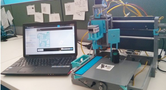
Squink PCB printer and Pick and Place

Prototyping circuits is still a pain. The typical process is to order your PCBs, await their arrival, hand assemble a board, and start testing. It’s time consuming, and typically takes at least a week to go from design to prototype.

The folks at BotFactory are working on fixing that with the Squink (Kickstarter warning). This device not only prints PCBs, but also functions as a pick and place. Rather than using solder, the device uses conductive glue to affix components to the substrate.

This process also allows for a wide range of substrates. Traditional FR4 works, but glass and flexible substrates can work too. They’re also working on using an insulating ink for multilayer boards.

While there are PCB printers out there, and the home etching process always works, building the board is only half the battle. Hand assembly using smaller components is slow, and is prone to mistakes. If this device is sufficiently accurate, it could let us easily prototype complex packages such as BGAs, which are usually a pain.

Of course it has its limitations. The minimum trace width is 10 mils, which is a bit large. Also at $2600, this is an expensive device to buy sight unseen. While it is a Kickstarter, it’d be nice to see an all in one device that can prototype circuits quickly and cheaply.

An Amazing DIY Single Board ARM Computer With BGA

DIY Single Board Computer ARM

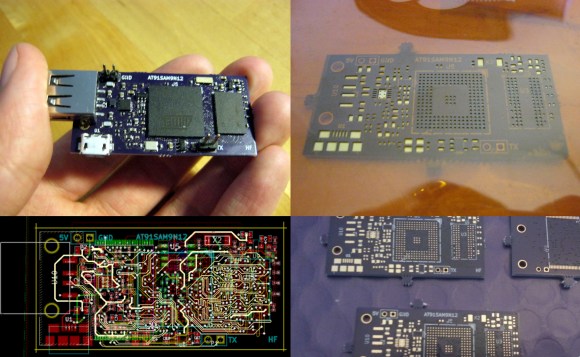
Typically, you buy a single board Linux computer. [Henrik] had a better idea, build his own ARM based single board computer! How did he do it? By not being scared of ball grid array (BGA) ARM processors.

Everyone loves the Raspberry Pi and Beagle Board, but what is the fun in buying something that you can build? We have a hunch that most of our readers stay clear of BGA chips, and for good reason. Arguably, one of the most important aspects of [Henrik’s] post is that you can easily solder BGAs with cheaply available tools. OSH Park provides the inexpensive high-quality PCBs, OSH Stencils provides the inexpensive stencils, and any toaster oven allows you to solder even the most difficult of components. Not only does he go over the PCB build, he also discusses the bootloader, u-boot, and how to get Linux running.

Everything worked out very well for [Henrik]. It’s a good thing too, cause we sure wouldn’t want to debug a PCB as complicated as this one. What projects have you built that use a BGA? Let us know how it went!

Shenzhen Tour And UnHuman Soldering Classes With DP

dp-hacker-camp

If you’re free the first week of April and don’t mind sitting on a plane for a looooong time you should check out the Hacker Camp that Dangerous Prototypes is planning. We’re sure you remember [Ian Lesnet] who is a Hackaday Alum, creator of the Bus Pirate, and geeky world traveler. Now’s your chance to try out what to him is a way of life.

The event is April 3-5 in Shenzhen, China. Although marketed as a “Hacker Camp”, to us it sounds more like training for those interested in running hardware companies that use the Shenzhen manufacturing district as the anchor of their supply chain. Part of the prep-work for the trip includes submitting board files which will be fabbed and ready for you on the first day. [Ian] and his crew will be your guides for the culture of the area; complete with meals and bar time. But there are also soldering workshops as part of the package. Don’t pooh-pooh the idea. This is unhuman soldering… BGA and QFN soldering instruction from the people who repair cellphones and other microelectronics.

This [Rick Steves] style adventure is the first that we remember hearing about that targets the open hardware community. But we must admit, it sounds like a lot more fun than a European river cruise!

[Thanks Akiba]

Hand Soldering BGA Wafer Chips

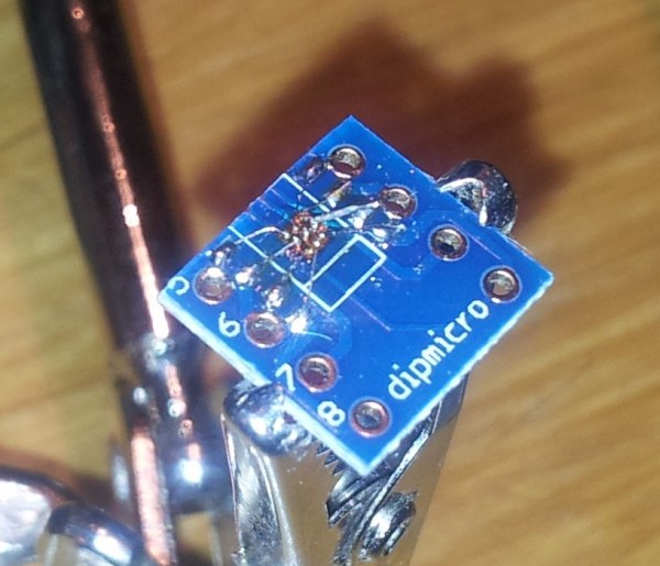
And here we’ve been complaining about Flat Pack No-Lead chips when this guy is prototyping with Ball Grid Array in a Wafer-Level Chip Scale Package (WLCSP). Haven’t heard that acronym before? Neither had we. It means you get the silicon wafer without a plastic housing in order to save space in your design. Want to use that on a breadboard. You’re crazy!

Eh, that’s just a knee jerk reaction. The wafer-level isn’t that unorthodox as far as manufacturing goes. It’s something like chip on board electronics which have that black blob of epoxy sealing them after the connections are made. This image shows those connections which use magnet wire on a DIP breakout board. [Jason] used epoxy to glue the wafer down before grabbing his iron. It took 90 minutes to solder the nine connections, but his second attempt cut that process down to just 20. After a round of testing he used more epoxy to completely encase the chip and wires.

It works for parts with low pin-counts. But add one row/column and you’re talking about making sixteen perfect connections instead of just nine.

BGA Rework Station

SMD components may be a little challenging for the home builder – even though the’re inordinately practical for homebrew PCBs – but if you play around with electronics and solder long enough, you’re eventually going to run into the horrors of BGA parts. Instead of convenient pins, BGA parts have tiny metallic balls on which solder is applied, a board is thrown through a reflow oven, and hopefully at the end, everything works. Sometimes these balls corrode or otherwise need to be reflowed. This isn’t an easy process, so [Edmar] came up with his own BGA rework station that costs much less than commercial offerings.

[Edmar]’s build began when he wanted to repair a graphics card. A common error on his Amilo XI2428 graphics card is having the small balls on the underside of the chip corrode, leaving the user with a non-functional graphics card. Towel trick notwithstanding, the easiest way to fix this error is to heat up the card to above the melting point of solder, removing the chip, and resoldering it with careful application of solder paste.

[Edmar]’s reflow station is made of an electric skillet for the bottom of the board, an infrared lamp for the top side of the board, and control circuitry constructed from an ATMega128, temperature sensors, and a huge power supply. The temperature is controlled via USB by a computer, allowing [Edmar] to set a temperature profile as recommended by the BGA chip’s data sheet.

Right now, removing a BGA chip works great, but [Edmar] is still working on the tech necessary to replace a BGA chip on a board.

Hand Soldering BGA Parts Should Be A Circus Act

Okay, we think it’s questionable when people say they have no problem soldering QFN packages, but BGA? Granted this chip has far fewer balls on it than many, but it’s still quite impressive that [Xevel] was able to solder this BGA breakout by hand.

The chip you see above is a TMP006 infrared temperature sensor from TI. [Xevel] picked up the part but didn’t want to break the bank when prototyping by buying a proper PCB to host it. There are only eight conductors on it, arranged in a grid with 0.5mm pitch. That didn’t seem to scare him off, as the video after the break shows him connecting each to a conductor on a hunk of stripboard.

[Xevel] mentions that this is a dead-bug style project. Usually you glue the part upside down when using that technique, but it needs line of sight to get an accurate temperature reading so he first cut a hole in the substrate. We’d bet he’s using wire-wrapping wire to make the connections. It’s a very fine solid core wire which is perfect for this kind of work.

Continue reading “Hand Soldering BGA Parts Should Be A Circus Act”