If you like your synthesizers glitchy, squawky, or simply quick-and-dirty, you won’t want to miss this week’s Hack Chat with Hackaday’s own [Elliot Williams], because he’ll be brain-dumping everything he knows about making music with 4000-series CMOS logic chips. Break out your breadboards!
One of the things that every student of digital electronics learns, is that every single logic function can be made from a combination of NAND gates. But nobody is foolhardy enough to give it a try, after all that would require a truly huge number of gates!
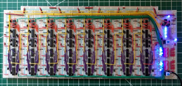
Someone evidently forgot to tell [Notbookies], for he has made a complete 8-bit ALU using only 4011B quad NAND gates on a set of breadboards, and in doing so has created a minor masterpiece with his wiring. It’s inspired by a series of videos from [Ben Eater] describing the construction of a computer with the so-called SAP (Simple As Possible) architecture. The 48 4011B DIP packages sit upon 8 standard breadboards, with an extra one for a set of DIP switches and LEDs, and a set of power busbar breadboards up their sides. He leaves us with the advice borne of bitter experience: “Unless your goal is building a NAND-only computer, pick the best IC for the job“.
We have covered countless processors and processor components manufactured from discrete logic chips over the years, though this makes them no less impressive a feat. The NedoNAND has been a recent example, a modular PCB-based design. TTL and CMOS logic chips made their debut over 50 years ago so you might expect there to be nothing new from that direction, however we expect this to be well of projects that will keep flowing for may years more.
Sometimes it seems like eBay is the world’s junk bin, and we mean that in the best possible way. The variety of parts available for a pittance boggles the mind sometimes, especially when the parts were once ordered in massive quantities but have since gone obsolete. The urge to order parts like these in bulk can be overwhelming, and sooner or later, you’ll find yourself with a fistful of old stuff but no idea how to put it to use.
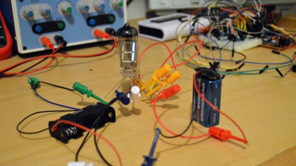
Case in point: the box of Russian surplus seven-segment vacuum fluorescent displays (VFDs) that [w_k_fay] had to figure out how to use. The result is a tutorial on quick and dirty VFD drivers that looks pretty handy. [w_k_fay] takes pains to point out that these are practical tips for putting surplus VFDs to work, as opposed to engineered solutions. He starts with tips on characterizing your surplus tubes in case you don’t have a pinout. A 1.5 V battery will suffice for the hot cathode, while a 9 V battery will turn on the segments. The VFDs can be treated much like a common cathode LED display, and a simple circuit driving the tube with a 4026 decade counter can be seen below. He also covers the challenges of driving VFDs from microcontrollers, and promises a full build of a frequency counter wherein the mysteries of multiplexing will be addressed.
Sounds like it’s time to stock up on those surplus VFDs and put them to work. For inspiration, take a look at this minimalist VFD clock, or perhaps mix VFDs with Nixies to satisfy your urge for all things glowy.
Don’t watch [Jason Hotchkiss]’s video if flashing lights or bleepy-bloopy synthesizer noises give you seizures. Do watch, however, if you’re interested in a big honeycomb-shaped LED matrix being driven at audio frequencies through a dedicated square-wave synthesizer that’s built in.
The LED panel in question is housed in a snazzy laser-cut, honeycomb-shaped bezel: a nice change from the standard square in our opinion. The lights are 1/2 watt (whoa!) whites, and the rows and columns are driven by transistor drivers that are in turn controlled by shift registers. We’re not entirely sure how the matrix is driven — we’d love to see a circuit diagram — but it looks like it’s some kind of strange, non-scanning mode where all of the column and row drives are on at once. Whatever, it’s art.
And it’s driven by logic chips making audio-frequency square waves. Two of these are fed into an LFSR and into an R-2R DAC and then into the shift registers. The output is chaos, but the audio and the visuals do seem to influence each other. It’s an audio-visual embodiment of some of my wildest Logic Noise fantasies. Pretty cool. Enjoy the video.
Like any Moore’s Law-inspired race, the megapixel race in digital cameras in the late 1990s and into the 2000s was a harsh battleground for every manufacturer. With the development of the smartphone, it became a war on two fronts, with Samsung eventually cramming twenty megapixels into a handheld. Although no clear winner of consumer-grade cameras was ever announced (and Samsung ended up reducing their flagship phone’s cameras to sixteen megapixels for reasons we’ll discuss) it seems as though this race is over, fizzling out into a void where even marketing and advertising groups don’t readily venture. What happened?
The Technology
A brief overview of Moore’s Law predicts that transistor density on a given computer chip should double about every two years. A digital camera’s sensor is remarkably similar, using the same silicon to form charge-coupled devices or CMOS sensors (the same CMOS technology used in some RAM and other digital logic technology) to detect photons that hit it. It’s not too far of a leap to realize how Moore’s Law would apply to the number of photo detectors on a digital camera’s image sensor. Like transistor density, however, there’s also a limit to how many photo detectors will fit in a given area before undesirable effects start to appear.
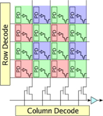
Image sensors have come a long way since video camera tubes. In the ’70s, the charge-coupled device (CCD) replaced the cathode ray tube as the dominant video capturing technology. A CCD works by arranging capacitors into an array and biasing them with a small voltage. When a photon hits one of the capacitors, it is converted into an electrical charge which can then be stored as digital information. While there are still specialty CCD sensors for some niche applications, most image sensors are now of the CMOS variety. CMOS uses photodiodes, rather than capacitors, along with a few other transistors for every pixel. CMOS sensors perform better than CCD sensors because each pixel has an amplifier which results in more accurate capturing of data. They are also faster, scale more readily, use fewer components in general, and use less power than a comparably sized CCD. Despite all of these advantages, however, there are still many limitations to modern sensors when more and more of them get packed onto a single piece of silicon.
While transistor density tends to be limited by quantum effects, image sensor density is limited by what is effectively a “noisy” picture. Noise can be introduced in an image as a result of thermal fluctuations within the material, so if the voltage threshold for a single pixel is so low that it falsely registers a photon when it shouldn’t, the image quality will be greatly reduced. This is more noticeable in CCD sensors (one effect is called “blooming“) but similar defects can happen in CMOS sensors as well. There are a few ways to solve these problems, though.
First, the voltage threshold can be raised so that random thermal fluctuations don’t rise above the threshold to trigger the pixels. In a DSLR, this typically means changing the ISO setting of a camera, where a lower ISO setting means more light is required to trigger a pixel, but that random fluctuations are less likely to happen. From a camera designer’s point-of-view, however, a higher voltage generally implies greater power consumption and some speed considerations, so there are some tradeoffs to make in this area.
Another reason that thermal fluctuations cause noise in image sensors is that the pixels themselves are so close together that they influence their neighbors. The answer here seems obvious: simply increase the area of the sensor, make the pixels of the sensor bigger, or both. This is a good solution if you have unlimited area, but in something like a cell phone this isn’t practical. This gets to the core of the reason that most modern cell phones seem to be practically limited somewhere in the sixteen-to-twenty megapixel range. If the pixels are made too small to increase megapixel count, the noise will start to ruin the images. If the pixels are too big, the picture will have a low resolution.
There are some non-technological ways of increasing megapixel count for an image as well. For example, a panoramic image will have a megapixel count much higher than that of the camera that took the picture simply because each part of the panorama has the full mexapixel count. It’s also possible to reduce noise in a single frame of any picture by using lenses that collect more light (lenses with a lower f-number) which allows the photographer to use a lower ISO setting to reduce the camera’s sensitivity.
Gigapixels!
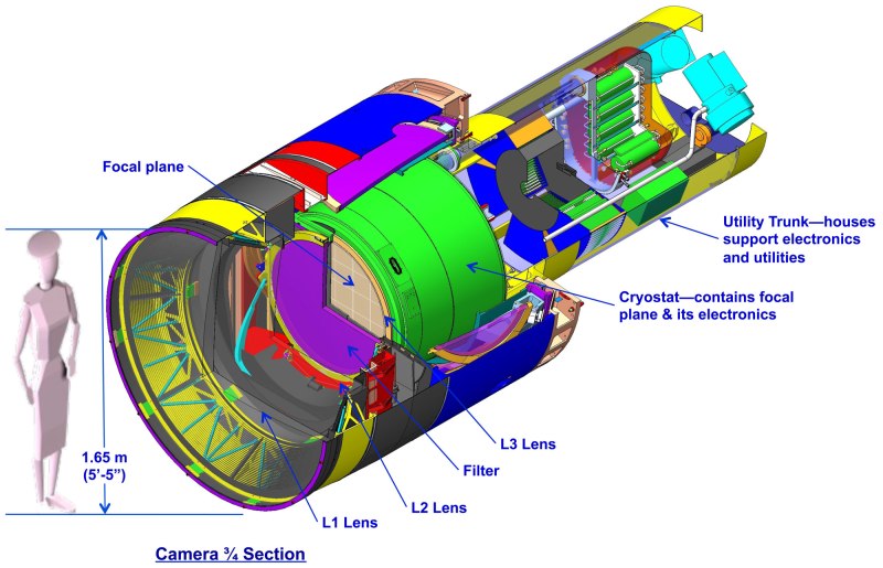
Of course, if you have unlimited area you can make image sensors of virtually any size. There are some extremely large, expensive cameras called gigapixel cameras that can take pictures of unimaginable detail. Their size and cost is a limiting factor for consumer devices, though, and as such are generally used for specialty purposes only. The largest image sensor ever built has a surface of almost five square meters and is the size of a car. The camera will be put to use in 2019 in the Large Synoptic Survey Telescope in South America where it will capture images of the night sky with its 8.4 meter primary mirror. If this was part of the megapixel race in consumer goods, it would certainly be the winner.
With all of this being said, it becomes obvious that there are many more considerations in a digital camera than just the megapixel count. With so many facets of a camera such as physical sensor size, lenses, camera settings, post-processing capabilities, filters, etc., the megapixel number was essentially an easy way for marketers to advertise the claimed superiority of their products until the practical limits of image sensors was reached. Beyond a certain limit, more megapixels doesn’t automatically translate into a better picture. As already mentioned, however, the megapixel count can be important, but there are so many ways to make up for a lower megapixel count if you have to. For example, images with high dynamic range are becoming the norm even in cell phones, which also helps eliminate the need for a flash. Whatever you decide, though, if you want to start taking great pictures don’t worry about specs; just go out and take some photographs!
(Title image: VISTA gigapixel mosaic of the central parts of the Milky Way, produced by European Southern Observatory (ESO) and released under Creative Commons Attribution 4.0 International License. This is a scaled version of the original 108,500 x 81,500, 9-gigapixel image.)
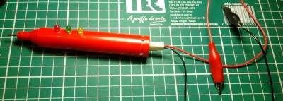
Logic probes are simple but handy tools that can be had for a couple of bucks. They may not be the sexiest pieces of test gear, nor the most versatile, but they have their place, and building your own logic probe is a great way to understand the tool’s strength and weaknesses.
[Jxnblk]’s take on the logic probe is based on a circuit by [Tony van Roon]. The design hearkens back to a simpler time and is based on components that would have been easy to pick up at any Radio Shack once upon a time. The logic section is centered on the venerable 7400 quad 2-input NAND gate in the classic 14-pin DIP format. The gates light separate LEDs for high and low logic levels, and a 555 timer chip in a one-shot configuration acts as a pulse stretcher to catch transients. The DIP packages lend themselves to quick and dirty “dead bug” construction, and the whole thing fits nicely into a discarded marking pen.
It’s a simple build and a nice form factor for a useful tool, but for an even slimmer package like an old syringe you’ll probably have to go with SMD components. And when you graduate from the simple logic probe, you might want to check out the capabilities of this smart probe.
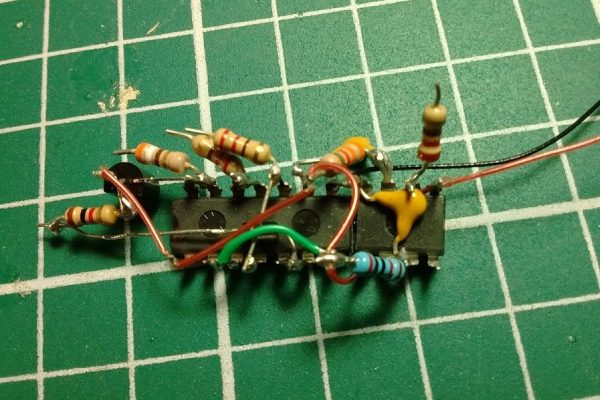
Looks like another shot has been fired in the simmering Coil Gun Control War. This time, [Great Scott] is taken to the discrete woodshed with a simplified and improved control circuit using a single CMOS chip and a few transistors. Where will it end? Won’t somebody think of the children?
The latest salvo is in response to [GreatScott]’s attempt to control a DIY coil gun with discrete logic, which in turn was a response to comments that he took the easy way out and used an Arduino in the original build. [Great Scott]’s second build was intended to justify the original design choice, and seemed to do a good job of explaining how much easier and better the build was with a microcontroller. Case closed, right?
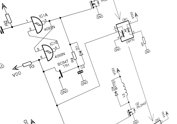
Nope. Embedded designer [fede.tft] wasn’t sure the design was even close to optimized, so he got to work — on his vacation, no less!’ He trimmed the component count down to a single CMOS chip (a quad Schmitt trigger NAND), a couple of switching transistors, the MOSFETs that drive the coils, and a few passives. The NANDs are set up as flip-flops that are triggered and reset by the projectile sensors, which are implemented as hardwired AND gates. The total component count is actually less than the support components on the original Arduino build, and [fede.tft] goes so far as to offer ideas for an alternative that does away with the switching transistors.
Even though [fede.tft] admits that [GreatScott] has him beat since he actually built both his circuits, hats off to him for showing us what can likely be accomplished with just a few components. We’d like to see someone implement this design, and see just how simple it can get.