Start Your Semiconductor Fab With This DIY Tube Furnace

Most of us are content to get our semiconductors from the usual sources, happily abstracting away the complexity locked within those little epoxy blobs. But eventually, you might get the itch to roll your own semiconductors, in which case you’ll need to start gearing up. And one of the first tools you’ll need is likely to be something like this DIY tube furnace.

For the uninitiated, [ProjectsInFlight] helpfully explains in the video below just what a tube furnace is and why you’d need one to start working with semiconductors. Perhaps unsurprisingly, a tube furnace is just a tube that gets really, really hot — like 1,200° C. In addition to the extreme heat, commercial furnaces are often set up to seal off the ends of the tube to create specific conditions within, such as an inert gas atmosphere or even a vacuum. The combination of heat and atmospheric control allows the budding fabricator to transform silicon wafers using chemical and physical processes.

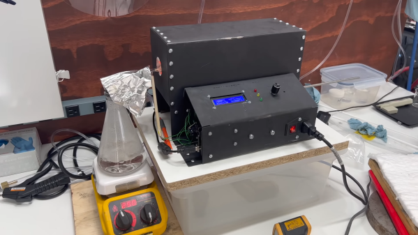
[ProjectsInFlight]’s tube furnace started with a length of heat-resistant quartz glass tubing and a small tub of sodium silicate refractory cement, from the plumbing section of any home store. The tube was given a thin coat of cement and dried in a low oven before wrapping it with nichrome wire. The wrapped tube got another, thicker layer of silicate cement and an insulating wrap of alumina ceramic wool before applying power to cure everything at 1,000° C. The cured tube then went into a custom-built sheet steel enclosure with plenty of extra insulation, along with an Arduino and a solid-state relay to control the furnace. The video below concludes with testing the furnace by growing a silicon dioxide coating on a scrap of silicon wafer. This was helped along by the injection of a few whisps of water vapor while ramping the furnace temperature up, and the results are easily visible.

[ProjectsInFlight] still needs to add seals to the tube to control the atmosphere in there, an upgrade we’ll be on the lookout for. It’s already a great start, although it might take a while to catch up to our friend [Sam Zeloof].

Continue reading “Start Your Semiconductor Fab With This DIY Tube Furnace”

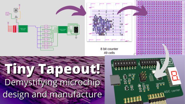
A sequence of pictures with arrows between each other. This picture shows a Wokwi (Fritzing-like) diagram with logic gates, going to a chip shot, going to a panel of chipsGA footprint on a KiCad PCB render with DIP switches and LEDs around the breakout. Under the sequence, it says: "Tiny Tapeout! Demystifying microchip design and manufacture"

Design Your Own Chip With TinyTapeout

When hackers found and developed ways to order PCBs on the cheap, it revolutionized the way we create. Accessible 3D printing brought us entire new areas to create things. [Matt Venn] is one of the people at the forefront of hackers designing our own silicon, and we’ve covered plenty of his research over the years. His latest effort to involve the hacker community, TinyTapeout, makes chip design accessible to newcomers – the bar is as low as arranging logic gates on a web browser page.

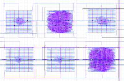
Six chip shots shown, with various densities of gates being used - some use a little, and some use a the entire area given.
Just six of the designs submitted, with varying complexity

For this, [Matt] worked with people like [Uri Shaked] of Wokwi fame, [Sylvain “tnt” Munaut], [jix], and a few others. Together, they created all the tooling necessary, and most importantly, a pipeline where your logic gate-based design in Wokwi gets compiled into a block ready to be put into silicon, with even simulations and compile-time verification for common mistakes. As a result, the design process is remarkably straightforward, to the point where a 9-year-old kid can do it. If you wanted, you could submit your Verilog, too!

The first round of TinyTapeout had a deadline in the first days of September and brought 152 entries together – just in time for an Efabless shuttle submission. All of these designs were put on a single instance of a chip, that will be fabbed in quantity, tested, soldered onto breakouts, and mailed out to individual participants. In this way, everyone will be getting everyone’s design, but thanks to the on-chip muxing hardware, they’re able to switch between designs using on-breakout DIP switches.

More after the break…

Continue reading “Design Your Own Chip With TinyTapeout”

Remoticon 2021 // Matt Venn Helps You Make ASICS

What would you make if you were given about ten square millimeters of space on a silicon wafer on a 130 nm process? That’s the exact question that the Open MPW program asks, and that [Matt Venn] has stepped up to answer. [Matt] came to Remoticon in 2020 to talk about his journey from nothing to his own ASIC, and he came back in 2021 to talk about what has happened in a year.

image of the metal layers of an IC
[maxiborga] has been making beautiful renders of his and others’ chip designs
We expected great designs, but the variety of exciting and wonderful designs that have been submitted we think exceeded our expectations. [Matt] goes through quite a few of them, such as an analog neuron, a RISC-V Arduino-compatible microprocessor, and a satellite transceiver. Perhaps an unexpected side effect has been the artwork. Since the designs are not under an NDA, anyone can take the design and transform it into something gorgeous.

Of course, all of this hardware design isn’t possible without an open toolchain. There is an SRAM generator known as OpenRAM that can generate RAM blocks for your design. Coriolis2 is an RTL to GDS tool that can do placement and routing in VLSI. Finally, FlexCell is a cell library that tries to provide standard functions in a flexible, customizable way that cuts down on the complexity of the layout. There are GitHub actions that can run tests and simulations on PRs to keep the chip’s HDL in a good state.

However, it’s not all roses, and there was an error on the first run (MPW1). Hold time violations were not detected, and the clock tree wasn’t correct. This means that the GPIO cannot be set up, so the designs in the middle could be working, but without the GPIO, it is tricky to determine. With a regular chip, that would be the end, but since [Matt] has access to both the layout and the design, he can identify the problem and come up with a plan. He’s planning on overriding the IO setup shift register with an auxiliary microcontroller. (Ed Note: [tnt] has been making some serious progress lately, summarized in this video.)

It is incredible to see what has come from the project so far, and we’re looking forward to future runs. If this convinces you that you need to get your own ASIC made, you should check out [Matt]’s “Zero to ASIC” course.

Continue reading “Remoticon 2021 // Matt Venn Helps You Make ASICS”

Garage Semiconductor Fab Gets Reactive-Ion Etching Upgrade

It’s a problem that few of us will likely ever face: once you’ve built your first homemade integrated circuit, what do you do next? If you’re [Sam Zeloof], the answer is clear: build better integrated circuits.

At least that’s [Sam]’s plan, which his new reactive-ion etching setup aims to make possible. While his Z1 dual differential amplifier chip was a huge success, the photolithography process he used to create the chip had its limitations. The chemical etching process he used is a bit fussy, and prone to undercutting of the mask if the etchant seeps underneath it. As its name implies, RIE uses a plasma of highly reactive ions to do the etching instead, resulting in finer details and opening the door to using more advanced materials.

[Sam]’s RIE rig looks like a plumber’s stainless steel nightmare, in the middle of which sits a vacuum chamber for the wafer to be etched. After evacuating the air, a small amount of fluorinated gas — either carbon tetrafluoride or the always entertaining sulfur hexafluoride — is added to the chamber. A high-voltage feedthrough provides the RF energy needed to create a plasma, which knocks fluorine ions out of the process gas. The negatively charged and extremely reactive fluorine ions are attracted to the wafer, where they attack and etch away the surfaces that aren’t protected by a photoresist layer.

It all sounds simple enough, but the video below reveals the complexity. There are a lot of details, like correctly measuring vacuum, avoiding electrocution, keeping the vacuum pump oil from exploding, and dealing with toxic waste products. Hats off to [Sam’s dad] for pitching in to safely pipe the exhaust gases through the garage door. This ties with [Huygens Optics]’s latest endeavor for the “coolest things to do with fluorine” award.

Continue reading “Garage Semiconductor Fab Gets Reactive-Ion Etching Upgrade”

Hackaday Links Column Banner

Hackaday Links: May 16, 2021

With the successful arrival of China’s first Mars lander and rover this week, and the relatively recent addition of NASA’s Perseverance rover and its little helicopter sidekick Ingenuity, Mars has collected a lot of new hardware lately. But while the new kids on the block are getting all the attention, spare a thought for the reliable old warhorse which has been plying Gale Crater for the better part of a decade now — Curiosity. NASA has been driving the compact-car-sized rover around Mars for a long time now, long enough to rack up some pretty severe damage to its six highly engineered wheels, thanks to the brutal Martian rocks. But if you think Curiosity will get sidelined as its wheels degrade, think again — the rover’s operators have a plan to continue surface operations that includes ripping off its own wheels if necessary. It’s a complex operation that would require positioning the wheel over a suitable rock and twisting with the steering motor to peel off the outer section of the wheel, leaving a rim to drive around on. JPL has already practiced it, but they predict it won’t be necessary until 2034 or so. Now that’s thinking ahead.

With all the upheaval caused by the ongoing and worsening semiconductor shortage, it might seem natural to expect that manufacturers are responding to market forces by building new fabs to ramp up production. And while there seems to be at least some movement in that direction, we stumbled across an article that seems to give the lie to the thought that we can build our way out of the crisis. It’s a sobering assessment, to say the least; the essence of the argument is that 20 years ago or so, foundries thought that everyone would switch to the new 300-mm wafers, leaving manufacturing based on 200-mm silicon wafers behind. But the opposite happened, and demand for chips coming from the older 200-mm wafers, including a lot of the chips used in cars and trucks, skyrocketed. So more fabs were built for the 200-mm wafers, leaving relatively fewer fabs capable of building the chips that the current generation of phones, IoT appliances, and 5G gear demand. Add to all that the fact that it takes a long time and a lot of money to build new fabs, and you’ve got the makings of a crisis that won’t be solved anytime soon.

From not enough components to too many: the Adafruit blog has a short item about XScomponent, an online marketplace for listing your excess inventory of electronic components for sale. If you perhaps ordered a reel of caps when you only needed a dozen, or if the project you thought was a done deal got canceled after all the parts were ordered, this might be just the thing for you. Most items offered appear to have a large minimum quantity requirement, so it’s probably not going to be a place to pick up a few odd parts to finish a build, but it’s still an interesting look at where the market is heading.

Speaking of learning from the marketplace, if you’re curious about what brands and models of hard drives hold up best in the long run, you could do worse than to look over real-world results from a known torturer of hard drives. Cloud storage concern Backblaze has published their analysis of the reliability of the over 175,000 drives they have installed in their data centers, and there’s a ton of data to pick through. The overall reliability of these drives, which are thrashing about almost endlessly, is pretty impressive: the annualized failure rate of the whole fleet is only 0.85%. They’ve also got an interesting comparison of HDDs and SSDs; Backblaze only uses solid-state disks for boot drives and for logging and such, so they don’t get quite the same level of thrash as drives containing customer data. But the annualized failure rate of boot SDDs is much lower than that of HDDs used in the same role. They slice and dice their data in a lot of fun and revealing ways, including by specific brand and model of drive, so check it out if you’re looking to buy soon.

And finally, you know that throbbing feeling you get in your head when you’re having one of those days? Well, it turns out that whether you can feel it or not, you’re having one of those days every day. Using a new technique called “3D Amplified Magnetic Resonance Imaging”, or 3D aMRI, researchers have made cool new videos that show the brain pulsating in time to the blood flowing through it. The motion is exaggerated by the imaging process, which is good because it sure looks like the brain swells enough with each pulse to crack your skull open, a feeling which every migraine sufferer can relate to. This reminds us a bit of those techniques that use special algorithms to detects a person’s heartbeat from a video by looking for the slight but periodic skin changes that occurs as blood rushes into the capillaries. It’s also interesting that when we spied this item, we were sitting with crossed legs, watching our upper leg bounce slightly in time with our pulse.

Continue reading “Hackaday Links: May 16, 2021”

Hackaday Links Column Banner

Hackaday Links: March 28, 2021

If you thought the global shortage of computer chips couldn’t get any worse, apparently you weren’t counting on 2021 looking back at 2020 and saying, “Hold my beer.” As if an impacted world waterway and fab fires weren’t enough to squeeze supply chains, now we learn that water restrictions could potentially impact chip production in Taiwan. The subtropical island usually counts on three or four typhoons a year to replenish its reservoirs, but 2020 saw no major typhoons in the region. This has plunged Taiwan into its worst drought since the mid-1960s, with water-use restrictions being enacted. These include a 15% reduction of supply to industrial users as well as shutting off the water entirely to non-industrial users for up to two days a week. So far, the restrictions haven’t directly impacted chip and display manufacturers, mostly because their fabs are located outside the drought zone. But for an industry where a single fab can use millions of gallons of water a day, it’s clearly time to start considering what happens if the drought worsens.

Speaking of the confluence of climate and technology, everyone problem remembers the disastrous Texas cold snap from last month, especially those who had to endure the wrath of the unusually brutal conditions in person. One such victim of the storm is Grady, everyone’s favorite YouTube civil engineer, who recently released a very good post-mortem on the engineering causes for the massive blackouts experienced after the cold snap. In the immediate aftermath of the event, we found it difficult to get anything approaching in-depth coverage on its engineering aspects — our coverage excepted, naturally — as so much of what we found was laden with political baggage. Grady does a commendable job of sticking to the facts as he goes over the engineering roots of the disaster and unpacks all the complexity of the infrastructure failures we witnessed. We really enjoyed his insights, and we wish him and all our friends in Texas the best of luck as they recover.

If you’re into the demoscene, chances are pretty good that you already know about the upcoming Revision 2021, the year’s big demoscene party. Like last year’s Revision, this will be a virtual gathering, but it seems like we’re all getting pretty used to that by now. The event is next weekend, so if you’ve got a cool demo, head over and register. Virtual or not, the bar was set pretty high last year, so there should be some interesting demos that come out of this year’s party.

Many of us suffer from the “good enough, move on” mode of project management, leaving our benches littered with breadboarded circuits that got far enough along to bore the hell out of us make a minimally useful contribution to the overall build. That’s why we love it when we get the chance to follow up on a build that has broken from that mode and progressed past the point where it originally caught our attention. A great example is Frank Olsen’s all-wood ribbon microphone. Of course, with magnets and an aluminum foil ribbon element needed, it wasn’t 100% wood, but it still was an interesting build when we first spied it, if a bit incomplete looking. Frank has fixed that in grand style by continuing the wood-construction theme that completes this all-wood replica of the iconic RCA Model 44 microphone. It looks fabulous and sounds fantastic; we can’t help but wonder how many times Frank glued his fingers together with all that CA adhesive, though.

Continue reading “Hackaday Links: March 28, 2021”

SkyWater PDK Hack Chat

Join us on Wednesday, September 16 at noon Pacific for the CNC on the SkyWater PDK Hack Chat with Tim “mithro” Ansell, Mohamed Kassem, and Michael Gielda!

We’ve seen incredible strides made in the last decade or so towards democratizing manufacturing. Things that it once took huge, vertically integrated industries with immense factories at their disposal are now commonly done on desktop CNC machines and 3D printers. Open-source software has harnessed the brainpower of millions of developers into tools that rival what industry uses, and oftentimes exceeds them. Using these tools and combining them with things like on-demand PCB production and contract assembly services, and you can easily turn yourself into a legit manufacturer.

This model of pushing manufacturing closer to the Regular Joe and Josephine only goes so far, though. Your designs have pretty much been restricted to chips made by one or the other big manufacturers, which means pretty much anyone else could come up with the same thing. That’s all changing now thanks to SkyWater PDK, the first manufacturable, open-source process-design kit. With the tools in the PDK, anyone can design a chip for the SkyWater foundry’s 130-nm process.  And the best part? It’s free — as in beer. That’s right, you can get an open-source chip built for nothing during chip manufacturing runs that start as early as this November and go through 2021.

We’re sure this news will stir a bunch of questions, so Tim Ansell, a software engineer at Google who goes by the handle “mithro” will drop by the Hack Chat to discuss the particulars. He’ll be joined by Mohamed Kassem, CTO and co-founder of efabless.com, and Michael Gielda, VP of Business Development at Antmicro. Together they’ll field your questions about this exciting development, and they’ll walk us through just what it takes to turn your vision into silicon.

join-hack-chatOur Hack Chats are live community events in the Hackaday.io Hack Chat group messaging. This week we’ll be sitting down on Wednesday, September 16 at 12:00 PM Pacific time. If time zones baffle you as much as us, we have a handy time zone converter.

Click that speech bubble to the right, and you’ll be taken directly to the Hack Chat group on Hackaday.io. You don’t have to wait until Wednesday; join whenever you want and you can see what the community is talking about.

Continue reading “SkyWater PDK Hack Chat”