This ESP32 Pico Wristwatch Has Plenty Of Potential

First hand-built prototype. Nurse! isopropyl alcohol, stat!

Prolific hacker [Sulfuroid] is a medical doctor by day, and an electronics hobbyist by night, and quite how he finds the time, we have no idea.

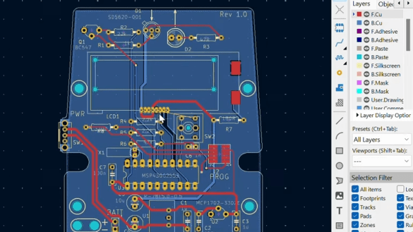
The project we want to highlight is an ESP32 based LED smart watch, which we’ll sure you’ll agree, looks pretty nicely developed so far, and [Sulfuroid] has bigger plans, as you may find, when you dig into the GitHub repo. This analog-style design uses four groups of 0603-sized LEDs, arranged circularly to indicate the passage of time, or anything else you fancy. Since there are four control buttons, a pancake vibration motor, as well as Wi-Fi and Bluetooth, the possibilities are endless.

In order to stand a hope of driving those 192 LEDs from a single ESP32-Pico-D4, it was necessary to use a multiplexed LED driver, courtesy of the Lumissil IS31FL3733 device, which can handle arrays up to 12 x 16 devices. This chip is one to remember, since it has some really nice features, such as global current control to reduce CPU overhead, automatic breathing loops for those fancy fade effects, and even includes a handy open/short detection function, so it can report back assembly problems, assisting in reworking your dodgy soldering!

Routing circular arrays is such a pain.

Power and interfacing are taken care of via USB-C, with a TP4054 single Li-Ion cell charger chip handling the battery. This is a Taiwanese clone of the popular LTC4054, but that chip may be a bit hard to get at the moment. There is the common-as-muck CP2104 USB chip dealing with the emulated serial port side of things, since for some reason, the ESP32 still does not support USB. The Pico-D4 does have RTC support, but [Sulfuroid] decided to use a DS3231M RTC chip instead. We noticed the touch functionality wasn’t broken out – that could be added easily in the next revision!

We’ve covered watches a lot, because who doesn’t want custom geek-wear! Here’s a slick one, a fun one with the brains on display, and finally one using charlieplexing to get the component count down.


Ultra Cheap PCB Wrenches Make Perfect Kit Accessory

Let’s make one thing abundantly clear. We do not, under any circumstances, recommend you replace your existing collection of wrenches with ones made out of PCBs. However, as creator [Ben Nyx] explains, they do make for an extremely cheap and lightweight temporary tool that would be perfect for distributing with DIY kits.

This clever open hardware project was spawned by [Ben]’s desire to pack an M3 wrench in with the kits for an ESP32-based kiln controller he’s developing. He was able to find dirt cheap screwdrivers from the usual import sites, but nobody seemed to stock a similarly affordable wrench. He experimented with 3D printing them, but in the end, found the plastic just wasn’t up to the task. Then he wondered how well a tiny wrench cut from a PCB would fare.

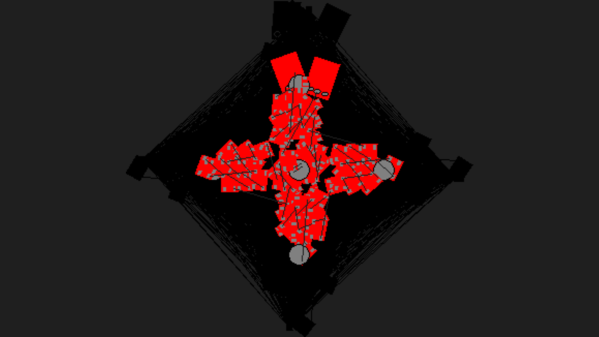
The answer, somewhat surprisingly, is pretty well. We wouldn’t advise you try to crank your lug nuts down with one, but for snugging up a couple nuts that hold down a control board, they work a treat. [Ben] came up with a panelized design in KiCad that allows 18 of the little wrenches to get packed into a 100 x 100 mm PCB suitable for production from popular online board houses. Manufactured from standard 1.6 mm FR4, they come out to approximately 10 cents a pop.

Since [Ben] has been kind enough to release his design under the MIT license, you’re free to spin up some of these wrenches either for your own kits or just to toss in the tool bag for emergencies. We’d love to see somebody adapt the design for additional sizes of nuts, or maybe figure out some way to nest them to sneak out a couple extra wrenches per board.

We’ve seen plenty of folks make cheap tools for themselves in the past, but projects that can produce cheap tools in mass quantities is uniquely exciting for a community like ours.

Continue reading “Ultra Cheap PCB Wrenches Make Perfect Kit Accessory”

KiCAD 6.0: What Made It And What Didn’t

I’ve been following the development of KiCAD for a number of years now, and using it as my main electronics CAD package daily for a the last six years or thereabouts, so the release of KiCAD 6.0 is quite exciting to an electronics nerd like me. The release date had been pushed out a bit, as this is such a huge update, and has taken a little longer than anticipated. But, it was finally tagged and pushed out to distribution on Christmas day, with some much deserved fanfare in the usual places.

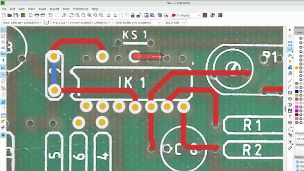
So now is a good time to look at which features are new in KiCAD 6.0 — actually 6.0.1 is the current release at time of writing due to some bugfixes — and which features originally planned for 6.0 are now being postponed to the 7.0 roadmap and beyond. Continue reading “KiCAD 6.0: What Made It And What Didn’t”

Advanced PCB Graphics With KiCAD 6 And Inkscape

There are many, many video tutorials about designing the functional side of PCBs, giving you tips on schematic construction, and layout tips. What is a little harder to find are tutorials on the graphical aspects, covering the process from creating artworks and how you can drive the tools to get them looking good on a PCB, leveraging the silkscreen, solder and copper layers to maximum effect. [Stuart Patterson] presents his guide for Advanced PCB Graphics in KiCAD 6.0 and Inkscape, (Video, embedded below) to help you on your way to that cool looking PCB build.

Silkscreen layers in yellow, solder mask opening in red

The first step is to get your bitmap, whether you create it yourself, or download it, and trace it into a set of vectors using the Inkscape ‘trace bitmap’ tool. If you started with an SVG or similar vector shape, then you can skip that stage.

Next simply create a PCB outline shape by deleting all the details that aren’t part of the outline. A little scaling here and there to get the dimensions correct and you’re done with the first part. [Stuart] has an earlier video showing that process.

The usability improvements in KiCAD 6.0 are many, but one greatly demanded feature is the ability to group objects, just like you do in Inkscape and any other vector graphics tool for that matter. That means you can simply import that SVG outline into the Edge.Cuts PCB layer and all the curves will be nicely tied together. Next you select the details you want for the silkscreen layer, solder mask removal layers and any non-circuit copper. In Inkscape it would be wise to use the layers feature to assign the different material types to a uniquely named layer, so they can be hidden for exporting. This allows you to handle silk, mask and copper PNG exports from a single master file, in addition to any vector details for outline, slots and holes.

Once you have PNG bitmap exports for the silk, mask etc. you need to create a footprint inside a board-specific library, using the KiCAD image converter tool. It was interesting to note that you can export a new image footprint from the tool and paste it straight into the footprint editor, and tweak all the visibility details at the same time. That will save some time and effort for sure. Anyway, we hope this little tutorial from [Stuart] helps, and we will be sure to bring you plenty more in the coming months.

Need some more help with KiCAD? Checkout this tutorial, and if you want a bit more power from the tool, you need some action plugins!

Continue reading “Advanced PCB Graphics With KiCAD 6 And Inkscape”

Schematic-o-matic

Tricked-Out Breadboard Automatically Draws Schematics Of Whatever You Build

When it comes to electronic design, breadboarding a circuit is the fun part — the creative juices flow, parts come and go, jumpers build into a tangled mess, but it’s all worth it when the circuit finally comes to life. Then comes the “What have I done?” phase, where you’ve got to backtrack through the circuit to document exactly how you built it. If only there was a better way.

Thanks to [Nick Bild], there is, in the form of the “Schematic-o-matic”, which aims to automate the breadboard documentation process. The trick is using a breadboard where each bus bar is connected to an IO pin on an Arduino Due. A program runs through each point on the breadboard, running a continuity test to see if there’s a jumper connecting them. A Python program then uses the connection list, along with some basic information about where components are plugged into the board, to generate a KiCad schematic.

[Nick] admits the schematics are crude at this point, and that it’s a bit inconvenient to remove some components, like ICs, from the breadboard first to prevent false readings. But this seems like one of those things where getting 80% of the work done automatically and worrying about the rest later is a big win. Plus, we can see a path forward to automatic IC probing, and even measurement of passive components too. But even as it is, it’s a great tool.

Continue reading “Tricked-Out Breadboard Automatically Draws Schematics Of Whatever You Build”

Slick Keyboard Built With PCB Magic

Sometimes a chance conversation leads you to discover something cool you’ve not seen before, and before you know it, you’re ordering parts for yet another hardware build. That’s what happened to this scribe the other day when chatting on some random discord, to QMK maintainer [Nick Brassel aka tzarc] about Djinn, a gorgeous 64-key split mechanical keyboard testbed. It’s a testbed because it uses the newest STM32G4x microcontroller family, and QMK currently does not have support for this in the mainline release. For the time being, [Nick] maintains a custom release, until it gets merged.

Hardware-wise, the design is fabulous, with a lot of attention to detail. We have individual per-key RGB LEDs, RGB underglow, a rotary encoder, a five-way tactile thumb switch, and a 240×320 LCD per half. The keyboard is based on a three PCB stack, two of which are there purely for structure. This slick design has enough features to keep a fair few of us happy.

Interestingly, when you look at the design files (KiCAD, naturally) [Nick] has chosen to take a mirrored approach to the PCB. That means the left and right sides are actually the same PCB layout. The components are populated on different sides of the PCB depending on which half you’re looking at! By mirroring footprints on both PCB sides, and hooking everything up in parallel, it’s possible to do it all with a single master layout.

This is a simple but genius idea that this scribe hadn’t come across before (the shame!) Secondarily it keeps costs down, as your typical Chinese prototyping house will not deal in PCB quantities below five, so you can make two complete keyboards on one order, rather than needing two orders to make five. (Yes, there are actually three unique PCBs, but we’re simplifying the situation, ok?)

Now, if only this pesky electronics shortage could abate a bit, and we could get the parts to build this beauty!

Obviously, we’ve covered many, many keyboards over the years. Here’s our own [Kristina’s] column all about the things. If you need a little help with your typing skills, this shocking example may be the one for you. If your taste is proper old-school clackers, there’s something for everyone.

Flip-Chip KiCad Templates

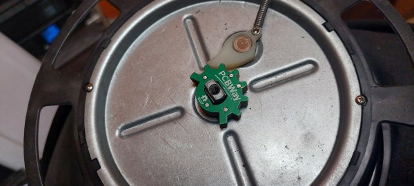
We like retro-computing and we like open source standards that allow easy project sharing. Vintage DEC computer enthusiast [Jay Logue] combines both of theseĀ in his recent project on GitHub, where he shares several KiCad templates for making your own Flip-Chip modules. Although named after the semiconductor packaging technique we are familiar with today, DEC Flip-Chips were introduced in 1964 as a modular electronics packaging system. These were used in many of DEC’s Programmable Data Processor (PDP) computers, beginning with the PDP-8 in 1965. DEC also had a Digital Laboratory Module family, which was a roll-your-own custom electronic system. The 1968 Digital Logic Handbook shows the available modules, and has the look and feel of the TTL Cookbook book which would come along six years later.

Flip-Chips came in a variety of sizes over the years: single-, double-, and quad-, and hex-height boards having standard- and extended-length. The PCB’s have 18 gold-plated fingers on one edge, later extended to 36 fingers double-sided, which plug into a backplane. Interconnections were typically wire-wrapped. A single height board is 127 x 62 mm (5 x 2-7/16 inches) with a labeled extractor bracket on one end. [Jay]’s repository has templates for five of the most popular variations, and making other sizes should be straightforward using these templates as a starting point.

Continue reading “Flip-Chip KiCad Templates”