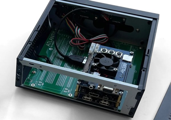
Playing classic games, whether they are games from the golden age of arcades or simply games from consoles that are long out of production, tends to exist on a spectrum. At one end is grabbing a game’s ROM file, finding an emulator, and kludging together some controls on a keyboard and mouse with your average PC. At the other is meticulously restoring classic hardware for the “true” feel of what the game would have felt like when it was new. Towards the latter end is emulating the hardware with an FPGA which the open-source MiSTer project attempts to do. This build, though, adds ATX capabilities for the retrocomputing platform. Continue reading “Classic Gaming With FPGA And ATX”→
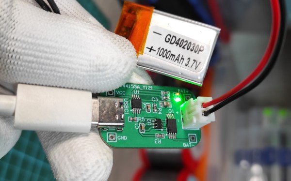
Lithium batteries have, nearly single-handedly, ushered in the era of the electric car, as well as battery energy storage of grid power and plenty of other technological advances not possible with older battery chemistries. There’s just one major downside: these lithium cells can be extremely finicky. If you’re adding one to your own project you’ll have to be extremely careful to treat them exactly how they are designed to be treated using something like this boilerplate battery protection circuit created by [DIY GUY Chris].
The circuit is based around the TP4056 integrated circuit, which handles the charging of a single lithium cell — in this design using supplied power from a USB port. The circuit is able to charge a cell based on the cell’s current charge state, temperature, and a model of the cell. It’s also paired with a DW01A chip which protects the cell from various undesirable conditions such as over-current, overcharge, and over-voltage.
The best thing about this design isn’t the design itself, but that [DIY GUY Chris] built the circuit schematic specifically to be easily copied into PCB designs for other projects, which means that lithium batteries can more easily be integrated directly into his other builds. Be sure to check out our primer on how to deal with lithium batteries before trying one of your own designs, though.
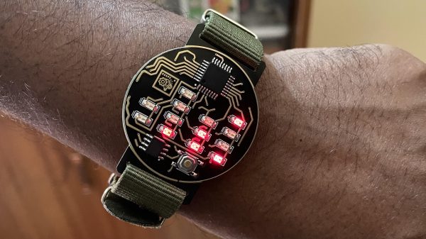
Most of us learn to read digital clocks first, which display the time in obvious numbers. Analog clocks are often learned later, with the hands taking our young brains a little longer to figure out. Once you’ve grown into a 1337h4XX0r, though, you’re ready to learn how to read a binary watch. Then you can build your own, just like [taifur] did.
The watch rocks a simplistic, bare bones design with the PCB acting as the body of the device itself. It’s not great for water resistance, or even incidental contact, but it’s a sharp look with the golden traces on display. The heart of the operation is a ATmega328P, as seen in the popular Arduino Uno, and it’s paired with a DS3231M real-time clock module to keep accurate time. 13 SMD LEDs are charged with displaying the time in binary format, with [taifur] choosing to spec a classic red color for the build. The watch is powered via a CR2032 coin cell, which you’re best advised not to swallow. So far, [taifur] has found the watch will last for over a month before the battery is tapped out.
It’s a fun build, and one that looks good when paired with a classic NATO watch strap in green. If, however, you desire a watch that definitely won’t last a month on a single coin cell, you can always build a Nixie watch instead. Video after the break.
Surface mount components have been a game changer for the electronics hobbyist, but doing reflow soldering right requires some way to evenly heat the board. You might need to buy a commercial reflow oven — you can cobble one together from an old toaster oven, after all — but you still need something, because it’s not like a PCB is going to solder itself. Right?
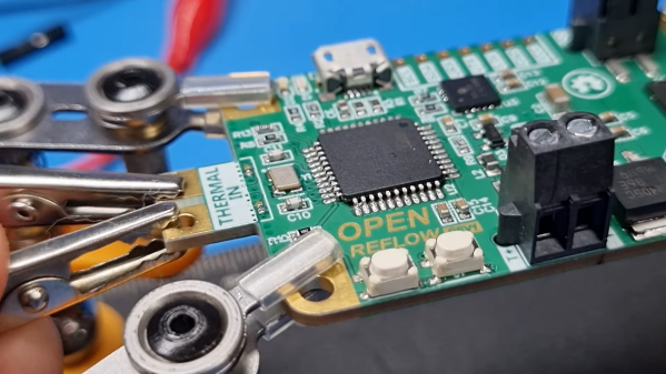
Wrong. At least if you’re [Carl Bugeja], who came up with a clever way to make his PCBs self-soldering. The idea is to use one of the internal layers on a four-layer PCB, which would normally be devoted to a ground plane, as a built-in heating element. Rather than a broad, continuous layer of copper, [Carl] made a long, twisting trace covering the entire area of the PCB. Routing the trace around vias was a bit tricky, but in the end he managed a single trace with a resistance of about 3 ohms.
When connected to a bench power supply, the PCB actually heats up quickly and pretty evenly judging by the IR camera. The quality of the soldering seems very similar to what you’d see from a reflow oven. After soldering, the now-useless heating element is converted into a ground plane for the circuit by breaking off the terminals and soldering on a couple of zero ohm resistors to short the coil to ground.
The whole thing is pretty clever, but there’s more to the story. The circuit [Carl] chose for his first self-soldering board is actually a reflow controller. So once the first board was manually reflowed with a bench supply, it was used to control the reflow process for the rest of the boards in the batch, or any board with a built-in heating element. We expect there will be some limitations on the size of the self-soldering board, though.
We really like this idea, and we’re looking forward to seeing more from [Carl] on this.
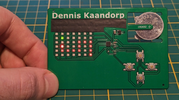
There’s no better way to introduce yourself than handing over a blinky PCB business card and challenging the recipient to a game of Connect Four. And if [Dennis Kaandorp] turns up early for a meeting, he can keep himself busy playing the ever popular game of Snake on his PCB business card.
The tabs are 19 mm long and 4 mm wide.
Quite wisely, [Dennis] kept his design simple, and avoided the temptation of feature creep. His requirements were to create a minimalist, credit card sized design, with his contact details printed on the silk legend, and some blinky LED’s.
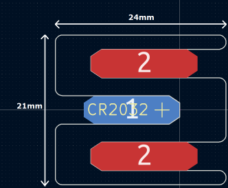
The tallest component on such a design is usually the battery holder, and he could not find one that was low-profile and cheap. Drawing inspiration from The Art of Blinky Business Cards, he used the 0.8 mm thin PCB itself as the battery holder by means of flexible arms.
Connect-Four is a two player game similar to tic-tac-toe, but played on a grid seven columns across and six rows high. This meant using 42 dual-colour LED’s, which would require a large number of GPIO pins on the micro-controller. Using a clever combination of matrix and charlieplexing techniques, he was able to reduce the GPIO count down to 13 pins, while still managing to keep the track layout simple.
It also took him some extra effort to locate dual colour, red / green LED’s with a sufficiently low forward voltage drop that could work off the reduced output resulting from the use of charlieplexing. At the heart of the business card is an ATtiny1616 micro-controller that offers enough GPIO pins for the LED matrix as well as the four push button switches.
His first batch of prototypes have given him a good insight on the pricing and revealed several deficiencies that he can improve upon the next time around. [Dennis] has shared KiCad schematic and PCB layout files for anyone looking to get inspired to design their own PCB business cards.
We’ve seen our share of custom PCBs here on Hackaday, but they aren’t always pretty. If you want to bring your PCB aesthetics up a notch, [Ian Dunn] has put together a guide for those wanting to get into PCB art.
There are plenty of tutorials about making a functional PCB, but finding information about PCB art can be more difficult. [Ian] walks us through the different materials available from PCB fabs and how the different layer features can affect the final aesthetic of a piece. For instance, while black and white solder mask are opaque, other colors are often translucent and affected by copper under the surface.
PCB design software can throw errors when adding decorative traces or components to a board that aren’t connected to any of the functional circuitry, so [Ian] discusses some of the tricks to avoid tripping up here. For that final artistic flair, component selection can make all the difference. The guide has recommendations on some of the most aesthetically pleasing types of components including how chips made in the USSR apparently have a little bit of extra panache.
It has become a bit of a running joke in the Hackaday community to suggest that a project could or should have been done with a 555 timer. [Tim] has rather taken this to heart with his latest Electronic Dice project, which uses three of the venerable devices.
If three seems like a lot of 555s to make an electronic die, then it may be worth considering that the last time we shared his project he was using 22 of them! Since then, [Tim] has been busy optimising his design, whilst keeping within the constraints of an old-school through-hole soldering kit.
Maybe the most surprising thing about this project is the purpose to which the NE555 devices are pressed. Rather than using them for their famous oscillation properties, they are in actual fact just being used as Schmitt Triggers to clean up the three-phase ring oscillator that is constructed from discrete transistors and passives.
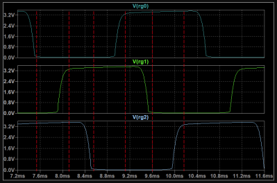
Simulation trace of the three-phase ring oscillator before Scmitt Trigger stages
The ring oscillator cleverly produces three phase-shifted square waves such that a binary combination of the three phases offers six unique states. Six being the perfect number for a dice throw, all that then remains is to figure out which LEDs need to be switched on in which state and wire them up accordingly.
To “roll” the dice, a push-button powers up the oscillator, and stops it again when it is released, displaying the random end-state on the LEDs.
It can be fun to see what can be done using old technology, and educational to try to optimise a design down to the fewest parts possible.
[Tim]’s earlier project is here if you want to see how the design has evolved. The documentation on both of these iterations is excellent and well worth a read.