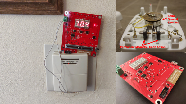
Laser Blasts Out High-Quality PCBs

With how cheap and how fast custom PCBs have gotten, it almost doesn’t make sense to roll your own anymore, especially when you factor in the messy etching steps and the less than stellar results. That’s not the only way to create a PCB, of course, and if you happen to have access to a 20-Watt fiber laser, you can get some fantastic homemade PCBs that are hard to tell from commercial boards.

Lucikly, [Saulius Lukse] of Kurokesu fame has just such a laser on hand, and with a well-tuned toolchain and a few compromises, he’s able to turn out 0.1-mm pitch PCBs in 30 minutes. The compromises include single-sided boards and no through-holes, but that should still allow for a lot of different useful designs. The process starts with Gerbers going through FlatCAM and then getting imported into EZCAD for the laser. There’s a fair bit of manual tweaking before the laser starts burning away the copper between the traces, which took about 20 passes for 0.035-mm foil on FR4. We have to admit that watching the cutting proceed in the video below is pretty cool.

Once the traces are cut, UV-curable solder resist is applied to the whole board. After curing, the board goes back to the laser for another pass to expose the pads. A final few passes with the laser turned up to 11 cuts the finished board free. We wonder why the laser isn’t used to drill holes; we understand that vias would be hard to connect to the other side, but it seems like through-hole components could be supported. Maybe that’s where [Saulius] is headed with this eventually, since there are traces that terminate in what appears to be via pads.

Whatever the goal, these boards are really slick. We usually see lasers used to remove resist prior to traditional etching, so this is a nice change.

Continue reading “Laser Blasts Out High-Quality PCBs”

Knockoff Kapton Nearly Sinks DIY Flex PCB Project

[TinkersProjects] experimented with making their own flexible PCB for LED modules inside a special fixture, and the end result was at least serviceable despite some problems. It does seem as though the issues can be at least partially blamed on some knockoff Kapton tape, which is what [TinkersProjects] used as a backing material.

Incomplete etching on this DIY flexible PCB, but still salvageable.

The approach was simple: after buying some copper foil and wide Kapton tape, simply stick the foil onto the tape and use the toner transfer method to get a PCB pattern onto the copper. From there, the copper gets etched away in a chemical bath and the process is pretty much like any other DIY PCB. However, this is also where things started to go wonky.

Etching was going well, until [TinkersProjects] noticed that the copper was lifting away from the Kapton tape. Aborting the etching process left a messy board, but it was salvageable. But another problem was discovered during soldering, as the Kapton tape layer deformed from the heat, as if it were a piece of heat shrink. This really shouldn’t happen, and [TinkersProjects] began to suspect that the “Kapton” tape was a knockoff. Switching to known-good tape was an improvement, but the adhesive left a bit to be desired because traces could lift easily. Still, in the end the DIY flexible PCB worked, though the process had mixed results at best.

Flexible PCBs have been the backbone of nifty projects like this self-actuating PoV display, so it’s no surprise that a variety of DIY PCB methods are getting applied to it.

Remoticon Video: KiCad To Blender PCB Renders

We seem to want our PCB design software to do everything these days, and it almost delivers. You can not only lay it all out, check electrical and design rules, and even spit out a bill of materials, but many PCB tools produce 3D models that are good enough to check parts clearance or are useful in designing enclosures. But when it comes to producing photorealistic output, whether for advertising or just for eye-candy, you might want to turn to 3D design tools.

In this workshop, Anool Mahidharia takes the output of KiCad’s VRML export, gets it rendering in Blender, and then starts tweaking the result until you’re almost not sure if it’s the real thing or a 3D model. He starts off with a board in KiCad, included in the project’s GitHub repo, and you can follow along through the basic import, or go all the way to copying the graphics off the top of an ATtiny85 and making sure that the insides of the through-plated holes match the tops.

If you don’t know Blender, maybe you don’t know how comprehensive a 3D modelling and animation tool it is. And with the incredible power comes a notoriously steep learning curve up a high mountain. Anool doesn’t even try to turn you into a Blender expert, but focuses on the tweaks and tricks that you’ll need to make good looking PCB renders. You’ll find general purpose Blender tutorials everywhere on the net, but if you want something PCB-specific, you’ve come to the right place.

Continue reading “Remoticon Video: KiCad To Blender PCB Renders”

Logitech Joystick Gets A Mechanical Sidekick

The mechanical keyboard rabbit hole is a deep one, and can swallow up as much money and time as you want to spend. If you’ve become spoiled on the touch and responsiveness of a Cherry MX or other mechanical switch, you might even start putting them on other user interfaces as well, such as this Logitech joystick that now sports a few very usable mechanical keys for the touch-conscious among us.

The Logitech Extreme 3D Pro that [ErkHal] and friend [HeKeKe] modified to accept the mechanical keys originally had a set of input buttons on the side, but these were unreliable and error-prone with a very long, inconsistent push. Soldering some mechanical switches directly on the existing board was a nice improvement, but the pair decided that they could do even better and rolled out an entire custom PCB to mount the keys more ergonomically. The switches are Kailh Choc V2 Browns and seem to have done a great job of improving the responsiveness of the joystick’s side buttons. If you want to spin up your own version, they’ve made the PCBs available on their GitHub page.

While [ErkHal] notes the switches aren’t the best and were only used since they were available, they certainly appear to work much better than what the joystick shipped with originally. In fact, we recently saw similar switches used to make a custom mechanical keyboard made for the PinePhone.

Printed Circuits, 1940s Style

A presentation this month by the Antique Wireless Museum brought British engineer and inventor John Sargrove (1906-1974) to our attention. If you’ve ever peeked inside old electronics from days gone by, you’ve no doubt seen point-to-point wiring and turret board construction. In the 60s and 70s these techniques eventually made way for printed circuit boards which we still use today. But Mr Sargrove was way ahead of his time, having already invented a process in the 1930s to print circuits, not just boards, onto Bakelite. After being interrupted by the war, he formed a company Electronic Circuit Making Equipment (ECME) and was building broadcast radio receivers on an impressive automatic production line.

Mr. Sargrove’s passion was making radios affordable for everyone. But to achieve this goal, he had to make large advances manufacturing technology. His technique of embedding not only circuit traces, but basic circuit elements like resistors, capacitors, and inductors directly into the substrate foresaw techniques being applied decades later in integrated circuit design.  He also developed a compact vacuum tube which could be used in all circuits of a radio, called an “All-stage Valve“. Equally important was his futuristic automatic factory, which significantly reduced the number of factory workers needed to make radios from 1500 to 50. Having completed the radio design, he was also developing a television receiver using the same concepts. Unfortunately, ECME was forced into liquidation when a large order from India was cancelled upon declaration of independence in 1947.

You really must watch the video below. There are many bits and pieces of modern factory automation which we still use today, yet their implementation using 1940s techniques and technology is fascinating. Further reading links after the video. Thanks to [Mark Erdle] for the tip.

Continue reading “Printed Circuits, 1940s Style”

Remoticon Video: How To Reverse Engineer A PCB

You hold in your hand a circuit board from a product you didn’t make. How does the thing work? What a daunting question, but it’s both solvable and approachable if you know what you’re doing. The good news is that Eric Schlaepfer knows exactly what he’s doing and boiled down the process of reverse engineering printed circuit boards into this excellent workshop. It was presented live during the 2020 Hackaday Remoticon, and the edited video, which you’ll find below, was just published. Slides for the talk have been published on the workshop project page.

Need proof that he has skills that we all want? Last year Eric successfully reverse-engineered the legendary Sound Blaster audio card and produced his own fully-functional drop-in replacement called the Snark Barker. And then re-engineered it to work with the ancient MCA bus architecture. Whoa.

Continue reading “Remoticon Video: How To Reverse Engineer A PCB”

Get Over Your Fears

Some projects are just too complex, that’s for sure. But I’d be willing to bet that some things you think are too difficult actually aren’t, and it may be that all you need to get over your personal hurdle is a good demonstration. Here come three cases in point.

I was looking at the new Raspberry Pi Compute Module last weekend. They have a whole bunch of high-speed traces: things like Gigabit Ethernet, HDMI, and those crazy-fast SDI serial camera interfaces. I have no experience in high-speed design and layout at all, and frankly it gives me the willies. But the Raspberries also shipped me an IO demo board, and concomitant KiCAD design files, with the review board. Looking at it, they were just wires — maybe pairwise length-matched and impedance controlled — but also just wires. Opening up the KiCAD board file and clicking on the traces just like I do with my own designs, I’m a lot less scared. That was a revelation for me.

In a great writeup of his experience building ten different Linux single-board-computers from scratch, Jay Carlson had a similar effect on me. I would never have considered breaking out the hotplate for some CPU-and-DRAM action, and I’ve never had to lay out a PCB with a high density BGA chip before either. I’m not quite into Dunning-Kruger territory yet; I still have a healthy respect for the layout intricacies in fanning out a tight BGA CPU into a DRAM. But Jay’s frank assessments of what is easy and what is hard make it all seem within the realm of the doable.

As Mike and I were talking on the podcast about Jay’s work, Mike came clean about his fear of BGAs. I’ve done enough reflow-plate soldering, with parts that have a lead pitch that’s a factor of two finer than the 0.8 mm pitch BGAs in question, so it doesn’t seem implausible to me. And I’m 100% sure Mike could pull it off too, but he is in need of a BGA guru. Any good hobbyist videos out there?

Being a nerdy type, I’m much more focused on the knowledge and the inspiration, but maybe the courage is equally important — at least I think I undervalue it. I don’t need to lay out HDMI lines, or build a from-scratch Linux box, but I am no longer afraid that I couldn’t, and that’s because I’ve seen detailed examples of fellow hackers who’ve done the same. I might not get it right on the first shot, but I’m not afraid to try, and I wouldn’t have said the same before looking over other folks’ shoulders. Forza e corragio!