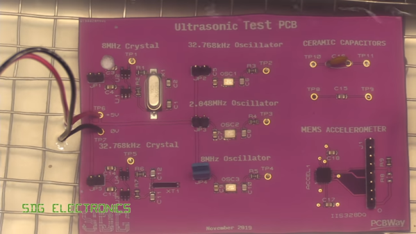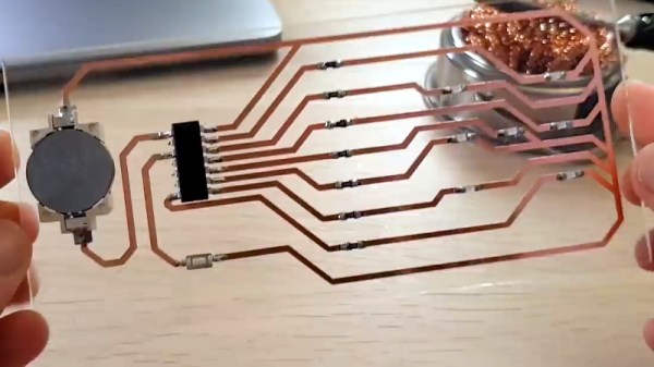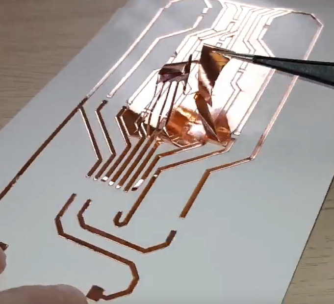
By now we are all used to the role of the printed circuit board in artwork, because of the burgeoning creativity in the conference and unofficial #BadgeLife electronic badge scenes. When the masters of electronic design tools turn their hand to producing for aesthetic rather than technical reasons, the results were always going to be something rather special.
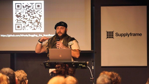
Nick Poole is an ace wrangler of electrons working for SparkFun, and as such is someone with an impressive pedigree when it comes to PCB design. Coming on stage sporting a beret with an awesome cap badge, his talk at the recent Hackaday Superconference concerned his experience in pushing the boundaries of what is possible in PCB manufacture. It was a primer in the techniques required to create special work in the medium of printed circuit boards, and it should be essential viewing for anybody with an interest in this field.
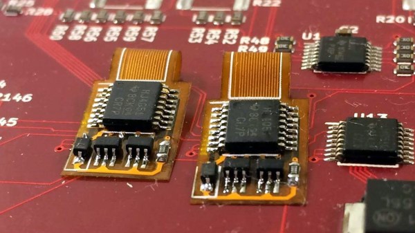
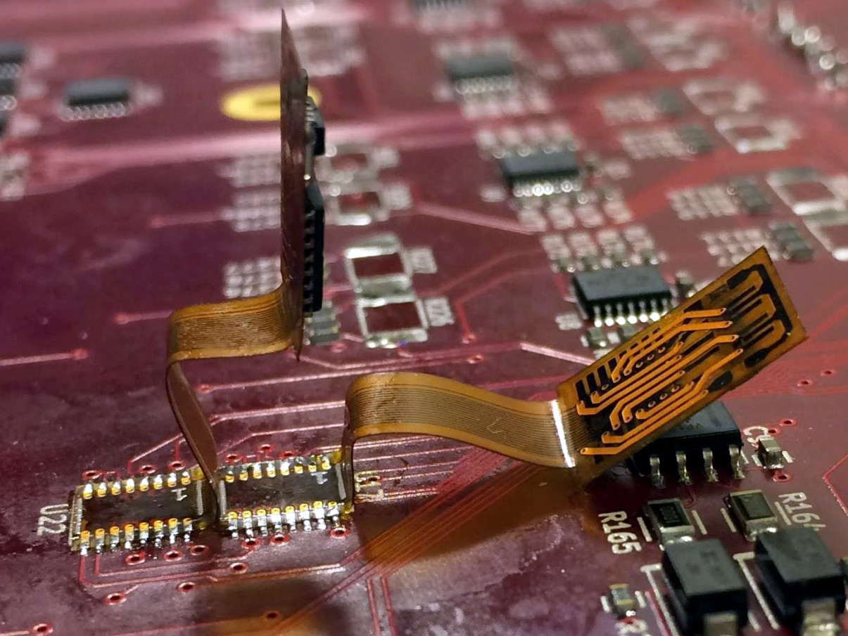
Though he starts with the basics of importing graphics into a PCB design package, the meat of his talk lies in going beyond the mere two dimensions of a single PCB into the third dimension either by creating PCBs that interlock, or by stacking boards.
Continue reading “Hackaday Superconference: Nick Poole On Boggling The Boardhouse”