Friday Hack Chat: Eagle One Year Later

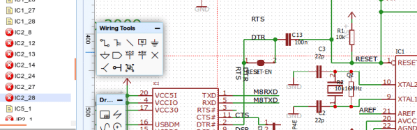
Way back in June of 2016, Autodesk acquired Cadsoft, and with it EagleCAD, the popular PCB design software. There were plans for some features that should have been in Eagle two decades ago, and right now Autodesk is rolling out an impressive list of features that include UX improvements, integration with MCAD and Fusion360, and push and shove routing.

Six months into the new age of Eagle, Autodesk announced they would be changing their licensing models to a subscription service. Where you could pay less than $100 once and hold onto version 6.0 forever, now you’re required to pay $15 every month for your copy of Eagle. Yes, there’s still a free, educational version, but this change to a subscription model caused much consternation in the community when announced.

For this week’s Hack Chat, we’re going to be talking about Eagle, one year in. Our guest for this Hack Chat is Matt Berggren, director of Autodesk Circuits, hardware engineer, and technologist that has been working on bringing electronic design to everyone. We’ll be asking Matt all about Eagle, with questions including:

  • What new features are in the latest edition of Eagle?
  • What’s on the Eagle wishlist?
  • What technical challenges arise when designing new features?
  • Where can a beginner find resources for designing PCBs in Eagle?

Join the chat to hear about new features in Eagle, how things are holding up for Eagle under new ownership, and how exactly the new subscription model for Eagle is going. We’re looking for questions from the community, so if you have a question for Matt or the rest of the Eagle team, put it on the Hack Chat event page.

If you’re wondering about how Altium and KiCad are holding up, or have any questions about these PCB design tools, don’t worry: we’re going to have Hack Chats with these engineers in the new year.

join-hack-chat

Our Hack Chats are live community events on the Hackaday.io Hack Chat group messaging. This Hack Chat is going down on noon, PST, Friday, December 15th. Time Zones got you down? Here’s a handy count down timer!

Click that speech bubble to the left, and you’ll be taken directly to the Hack Chat group on Hackaday.io.

You don’t have to wait until Friday; join whenever you want and you can see what the community is talking about.

EasyEDA Two Years Later

Some people want everything on the cloud, while others refuse to put even the smallest scrap of data on the Internet. Most of us fall somewhere in between. A few years ago, we talked about a few cloud-based PCB layout programs including one called EasyEDA. We were impressed because it was a full package: schematic capture, simulation, and PCB layout. It was free to use, although they would give you a quote for producing your boards, though you were under no obligation to buy them. Of course things change in two years, so if you are curious how EasyEDA is doing, [Yahya Tawil] posted an in-depth review.

Some of the new features include an autorouter and the ability to order parts from a BOM directly, not just PCBs. The cloud aspect is handy, not only because you don’t have to install and update software to use it anywhere, but because it is very natural to collaborate with others on projects. We did notice, though, that the autorouter can run in the cloud, or you can download and run it local because it apparently loads the server significantly.

Continue reading “EasyEDA Two Years Later”

Retrotechtacular: Circuit Boards The Tektronix Way

Printed circuit boards are a fundamental part of both of commercial electronic equipment and of the projects we feature here on Hackaday. Many of us have made our own, whether done so from first principles with a tank of etchant, or sent off as a set of Gerbers to a PCB fab house.

To say that the subject of today’s Retrotechtacular is the manufacture of printed circuit boards might seem odd, because there is nothing archaic about a PCB, they’re very much still with us. But the film below the break is a fascinating look at the process from two angles, both for what it tells us about how they are still manufactured, and how they were manufactured in 1969 when it was made.

Board artwork laid out at four-times actual size

Tektronix were as famous for the manufacturer of particularly high quality oscilloscopes back then as they are now. The Tektronix ‘scopes of the late 1960s featured several printed circuit boards carrying solid-state electronics, and were manufactured to an extremely high standard. The film follows the manufacturing process from initial PCB layout to assembled board, with plenty of detail of all production processes.

In 2017 you would start a PCB design in a CAD package, but in 1969 the was incredibly manual. Everything was transcribed by hand from a paper schematic to transparent film. Paper mock-ups of component footprints four times larger than actual size are placed on a grid, and conductors drawn in pencil on an overlaid piece of tracing paper. Then the pads and pattern of tracks are laid out using black transfers and tape on sheets of film over the tracing paper, one each for top and bottom of the board. A photographic process reduces them to production size onto film, from which they can be exposed and etched in the same way that you would in 2017.

Pantograph drilling machine uses a manually moved styuls on a template to drill six boards at once

Most of the physical process of creating a PCB has not changed significantly since 1969. We are shown the through-plating and gold plating processes in detail, then the etching and silkscreening processes, before seeing component installation and finally wave soldering.

What are anachronistic though are some of the machines, and the parts now robotised that were done in 1969 by hand. The PCB drilling is done by hand with a pantograph drill for small runs, but for large ones a fascinating numerically-controlled drilling rig is used, controlled by punched tape without a computer in sight. Component placement is all by hand, and the commentator remarks that it may one day be done by machine.

The film remains simultaneously an interesting look at PCB production and a fascinating snapshot of 1960s manufacturing. It’s probable that many of the Tek ‘scopes made on that line are still with us, they’re certainly familiar to look at from our experience at radio rallies.

Continue reading “Retrotechtacular: Circuit Boards The Tektronix Way”

Entry-Level 3D Printer Becomes Budget PCB Machine

A funny thing happened on [Marco Rep]’s way to upgrading his 3D printer. Instead of ending up with a heated bed, his $300 3D printer can now etch 0.2-mm PCB traces. And the results are pretty impressive, all the more so since so little effort and expense were involved.

The printer in question is a Cetus3D, one of the newer generation of affordable machines. The printer has nice linear bearings but not a lot of other amenities, hence [Marco]’s desire to add a heated bed. But hiding beneath the covers was a suspicious transistor wired to a spare connector on the print head; a little sleuthing and a call to the factory revealed that the pin is intended for accessory use and can be controlled from G-code. With a few mods to the cheap UV laser module [Marco] had on hand, a printed holder for the laser, and a somewhat manual software toolchain, PCBs with 0.2-mm traces were soon being etched. The video below shows that the printer isn’t perfect for the job; despite the smooth linear bearings, the low mass of the printer results in vibration that shows up as wavy traces. But the results are more than acceptable, especially for $330.

This isn’t [Marco]’s first budget laser-etching rodeo. He recently tried the same thing using a cheap CNC laser engraver with similar results. That was a $200 dedicated engraver, this is a $300 3D printer with a $30 laser. It seems hard to lose at prices like these.

Continue reading “Entry-Level 3D Printer Becomes Budget PCB Machine”

Making An Arduino Shield PCB With Fritzing

[Allan Schwartz] decided to document his experience using Fritzing to design, fabricate, and test a custom Arduino shield PCB, and his step-by-step documentation makes the workflow very clear. Anyone who is curious or has been looking for an opportunity to get started will find [Allan]’s process useful to follow. The PCB in question has two shift registers, eight LEDs, eight buttons, and fits onto an Arduino; it’s just complex enough to demonstrate useful design features and methods while remaining accessible.

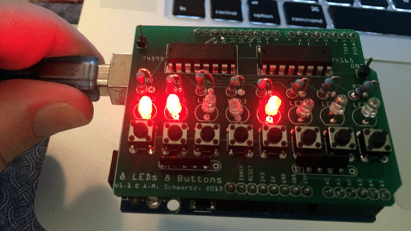
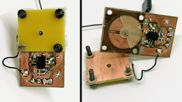
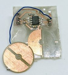
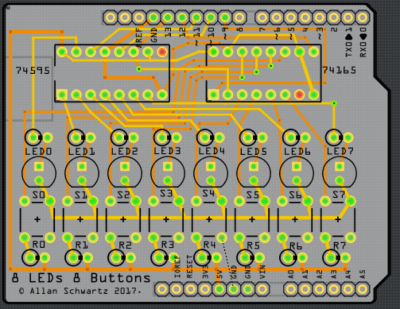
[Allan] starts with a basic breadboard design, draws a schematic, prototypes the circuit, then designs the PCB and orders it online, followed by assembly and testing. [Allan] had previously taught himself to use Eagle and etched his own PCBs via the toner transfer method, but decided to use Fritzing instead this time around and found it helpful and easy to use.

About a year ago we saw Fritzing put through its paces for PCB design, and at the time found that it didn’t impress much from an engineering perspective. Regardless, as a hobbyist [Allan] found real value in using Fritzing for his project from beginning to end; he documented both the process and his observations in order to help others, and that’s wonderful.

DIY Capacitive Rotational Encoder On The Cheap With FR4

Rotary encoders are critical to many applications, even at the hobbyist level. While considering his own rotary encoding needs for upcoming projects, it occurred to [Jan Mrázek] to try making his own DIY capacitive rotary encoder. If successful, such an encoder could be cheap and very fast; it could also in part be made directly on a PCB.

First prototype, two etched plates with transparent tape as dielectric material. Disc is 15 mm in diameter.

The encoder design [Jan] settled on was to make a simple adjustable plate capacitor using PCB elements with transparent tape as the dielectric material. This was used as the timing element for a 555 timer in astable mode. A 555 in this configuration therefore generates a square wave that changes in proportion to how much the plates in the simple capacitor overlap. Turn the plate, and the square wave’s period changes in response. Response time would be fast, and a 555 and some PCB space is certainly cheap materials-wise.

The first prototype gave positive results but had a lot of problems, including noise and possibly a sensitivity to temperature and humidity. The second attempt refined the design and had much better results, with an ESP32 reliably reading 140 discrete positions at a rate of 100 kHz. It seems that there is a tradeoff between resolution and speed; lowering the rate allows more positions to be reliably detected. There are still issues, but ultimately [Jan] feels that high-speed capacitive encoders requiring little more than some PCB real estate and some 555s are probably feasible.

This project is a reminder that FR4 (whether copper-clad, etched, or blank) shows up in clever applications: copper tape and blank FR4 can be used to quickly prototype RF filters, PocketNC built an entire small CNC tool around FR4, and our own [Voja] wrote a full guide on making beautiful enclosures from FR4.

More Homemade PCB Tinning

[Marko] styles himself as a crazy chemist. His video showing a fast tin plating solution for PCBs (YouTube, see below) doesn’t seem so crazy. We will admit, though, it uses some things that you might have to search for.

The formula calls for stannous chloride — you could probably make this by dissolving tin in hydrochloric acid. There’s also thiourea — the main chemical in silver-cleaning dips like Tarn-X. Sulphuric acid and deionized water round out the recipe.

Continue reading “More Homemade PCB Tinning”