Binary Wristwatch

Open Source Binary Wristwatch Is Professional Quality

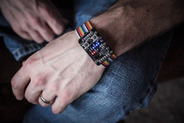
If you want to proclaim to the world that you’re a geek, one good way to go about it is to wear a wristwatch that displays the time in binary. [Jordan] designs embedded systems, and he figured that by building this watch he could not only build up his geek cred but also learn a thing or two about working with PIC microcontrollers for low power applications. It seems he was able to accomplish both of these goals.

The wristwatch runs off of a PIC18F24J11 microcontroller. This chip seemed ideal because it included a built in real-time clock and calendar source. It also included enough pins to drive the LEDs without the need of a shift register. The icing on the cake was a deep sleep mode that would decrease the overall power consumption.

The watch contains three sets of LEDs to display the information. Two green LEDs get toggled back and forth to indicate to the user whether the time or date is being displayed. When the time is being displayed, the green LED toggles on or off each second. The top row of red LEDs displays either the current hour or month. The bottom row of blue LEDs displays the minutes or the day of the month. The PCB silk screen has labels that help the user identify what each LED is for.

The unit is controlled via two push buttons. The three primary modes are time, date, and seconds. “Seconds” mode changes the bottom row of LEDs so they update to show how many seconds have passed in the current minute. [Jordan] went so far as to include a sort of animation in between modes. Whenever the mode is changed, the LED values shift in from the left. Small things like that really take this project a step further than most.

The board includes a header to make it easy to reprogram the PIC. [Jordan] seized an opportunity to make extra use out of this header. By placing the header at the top of the board, and an extra header at the bottom, he was able to use a ribbon cable as the watch band. The cable is not used in normal operation, but it adds that extra bit of geekiness to an already geeky project.

[Jordan] got such a big response from the Internet community about this project that he started selling them online. The only problem is he sold out immediately. Luckily for us, he released all of the source code and schematics on GitHub so we can make our own.

Deconstructing PCBs

The surest way to reverse engineer a circuit is to look at all the components, all the traces between these components, and clone the entire thing. Take a look at a PCB some time, and you’ll quickly see a problem with this plan: there’s soldermask hiding all the traces, vias are underneath components, and replicating a board from a single example isn’t exactly easy. That’s alright, because [Joe Grand] is here to tell you how to deconstruct PCBs one layer at a time.

Most of this work was originally presented at DEFCON last August, but yesterday [Joe] put up a series of YouTube videos demonstrating different techniques for removing soldermask, delayering multi-layer boards, and using non-destructive imaging to examine internal layers.

If you’re dealing with a two-layer board, the most you’ll have to do is remove the soldermask. This can be done with techniques ranging from a fiberglass scratch brush, to laser ablation, to a dremel flapwheel. By far the most impressive and effective ways to take the solder mask off of PCBs is the way the pros do it: chemically. A bath in Magnastrip 500 or Ristoff C-8 results in perfectly stripped boards and a room full of noxious chemicals. It makes sense; this is what PCB houses use when they need to remove solder mask during the fabrication process.

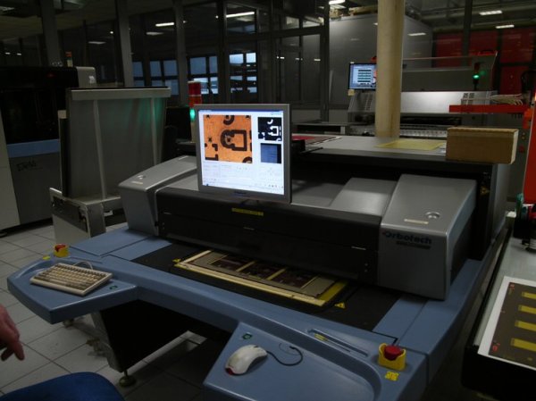
Removing a solder mask will get you the layout of a two-layer board, but if you’re looking at deconstructing multi-layer boards, you’ll have to delaminate the entire board stack to get a look at the interior copper layers. By far the most impressive way of doing this is with a machine that can only be described as gently violent, but passive, imaging techniques such as X-rays, CT scanners and other sufficiently advanced technology will also do the trick. Acoustic microscopy, or  Acoustic Micro Imaging, was, however, unsuccessful. It does look cool, though.

Thanks [Morris] for the tip.

Continue reading “Deconstructing PCBs”

Checking Populated PCB Clearance With A 3D Printer

Laying out one PCB, sending it out to a fab, stuffing it with components, and having the whole thing actually work when you’re done is a solved problem. Doing the same thing and having it plug in to another PCB… well, that’s a bit harder. Forget about building a PCB and having it fit inside an enclosure the first time.

The usual solution to this problem is printing the board to be fabbed on a piece of paper, take some calipers, and measure very, very carefully. Extra points for sticking a few components you’re worried about to the paper before lining the mechanical prototype up to the existing board. [N8VI] over at the i3 Detroit hackerspace had a better idea – print the whole thing out on a 3D printer.

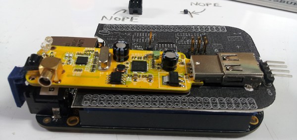
[N8VI] is working on a software defined radio cape for a BeagleBone. He was a bit concerned about a few caps getting in the way of a board stack. This was tested by printing out a bit of plastic in the shape of the new board, adding header spacers and parts that might be troublesome.

While the idea is great, there’s not much in the way of a software solution or a toolchain to make plastic copies of completed boards. We know rendering 3D objects from KiCAD is rather easy, but there aren’t many tools available for those of us who are still stuck with Eagle. If you know of a way to print populated boards, drop a note in the comments.

Toner Transfer And Packing Tape

The toner transfer process of producing PCBs has evolved tremendously over the last few years. It started out by printing PCB layouts onto magazines with a laser printer, then some clever people figured out that glossy inkjet photo paper would work just as well. Now there’s a new substrate for you – packing tape – and it seems to work pretty well.

[David] was designing a cheap board for a robot kit for a workshop and needed 100 tiny PCBs. They were simple boards, and perfectly suited for home PCB manufacturing. He started off by printing directly onto glossy magazine paper, but this wasn’t an ideal solution. During one run, some of the toner landed on the packaging tape he was using to secure the boards. A bit of serendipity came into play and [David] discovered packaging tape is usable in the toner transfer process.

The technique is simple enough: put some packaging tape on a piece of paper, print a board layout (reversed!) on a laser printer, and go through the usual clothes iron/laminator/etching process. [David] is actually using a hair straightener for transferring the toner over to the copper clad board – interesting, and in a pinch you can use the same tool for reflowing SMD components.

Valentine Heart

Animated LED Valentine Heart

With only a week left until Valentine’s day, [Henry] needed to think on his feet. He wanted to build something for his girlfriend but with limited time, he needed to work with what he had available. After scrounging up some parts and a bit of CAD work, he ended up with a nice animated LED Valentine heart.

[Henry] had a bunch of WS2812 LEDs left over from an older project. These surface mount LED’s are very cool. They come in a small form factor and include red, green, and blue LEDs all in a single package. On top of that, they have a built-in control circuit which makes each LED individually addressable. It’s similar to the LED strips we’ve seen in the past, only now the control circuit is built right into the LED.

Starting with the LEDs, [Henry] decided to build a large animated heart. Being a stickler for details, he worked out the perfect LED placement by beginning his design with three concentric heart shapes. The hearts were plotted in Excel and were then scaled until he ended up with something he liked. This final design showed where to place each LED.

The next step was to design the PCB in Altium Designer. [Henry’s] design is two-sided with large copper planes on either side. He opted to make good use of the extra copper surface by etching a custom design into the back with his girlfriend’s name. He included a space for the ATMega48 chip which would be running the animations. Finally, he sent the design off to a fab house and managed to get it back 48 hours later.

After soldering all of the components in place, [Henry] programmed up a few animations for the LEDs. He also built a custom frame to house the PCB. The frame includes a white screen that diffuses and softens the light from the LEDs. The final product looks great and is sure to win any geek’s heart. Continue reading “Animated LED Valentine Heart”

Circuit Love With Multicolor Solder Masks

The cheapest PCBs – and therefore most common – are green solder mask with white silkscreen. It works, but it’s also incredibly boring. This is the way things were done up until a few years ago with the explosion of board houses trying to compete for your Yuan, and now getting a red, yellow, black, blue, green, and even OSH purple is possible. This doesn’t mean multiple solder masks aren’t possible, as [Saar] demonstrates with his demonstration of multicolor solder masks and circuit love.

We’ve seen a lot of [Saar]’s designs, including a mixing desk, a cordwood puzzle, and an engineer’s emergency business card, but so far his artistic pieces have been decidedly monochromatic. For this build, [Saar] teamed up with Eurocircuits to create a board that exploits their capabilities.

Althought Eurocircuits has PCB PIXture, a tool for putting graphics on PCBs, [Saar] made this with his own tool, PCBmodE.  The design of both the red and yellow variants are abstract, and only meant to be a demonstration of what can be done with multicolor solder mask. It looks great with five backlit LEDs, and with an acrylic top and bottom, makes a great coaster or art piece.

We like [Saar’s] work so much that we put his Cordwood puzzle in the Hackaday Store.

Circuit Plotting With An HP Plotter

Over the last few years we’ve seen a few commercial products that aim to put an entire PCB fab line on a desktop. As audacious as that sounds, there were a few booths showing off just that at CES last week, with one getting a $50k check from some blog. [Connor] and [Feiran] decided to do the hacker version of a PCB printer: an old HP plotter converted to modern hardware with a web interface with a conductive ink pen.

The plotter in question is a 1983 HP HIPLOT DMP-29 that was, like all old HP gear, a masterpiece of science and engineering. These electronics were discarded (preserved may be a better word) and replaced with modern hardware. The old servo motors ran at about 1.5A each, and a standard H-Bridge chip and beefy lab power supply these motors were the only part of the original plotter that were reused. For accurate positioning, a few 10-turn pots were duct taped to the motor shafts and fed into the ATMega1284p used for controlling the whole thing.

One of the more interesting aspects of the build is the web interface. This is a small JavaScript app that is capable of drawing lines on the X and Y axes and sends the resulting coordinates from a server to the printer. It’s very cool, but not as cool as the [Connor] and [Feiran]’s end goal: using existing Gerber files to draw some traces. They’re successfully parsing Gerber files, throwing out all the superfluous commands (drills, etc), and plotting them in conductive ink.

The final iteration of hardware wasn’t exactly what [Connor] and [Feiran] had in mind, but that’s mostly an issue with the terrible conductivity of the conductive ink. They’ve tried to fix this by running the pen over each line five times, but that introduces some backlash. This is the final project for an electrical engineering class, so we’re going to say that’s alright.

Video below.

Continue reading “Circuit Plotting With An HP Plotter”