Last time on Circuit VR, we looked at creating a very simple common emitter amplifier, but we didn’t talk about how to select the capacitor values, or much about why we wanted them. We are going to look at that this time, as well as how to use a second transistor in an emitter follower (or common collector) configuration to stiffen the amplifier’s ability to drive an output load.
Several readers wrote to point out that I’d pushed the Ic value a little high for a 2N2222. As it turns out, at least one of the calculations in the comments was a bit high. However, I’ve updated the post at the end to explore what was in the comments, and talk a bit more about how you compute power dissipation with or without LTSpice. If you read that post, you might want to jump back and pick up the update. Continue reading “Circuit VR: A Tale Of Two Transistors”→
Sometimes I wish FETs had become practical before bipolar transistors. A FET is a lot more like a tube and amplifies voltages. Bipolar transistors amplify current and that makes them a bit harder to use. Recently, [Jenny List] did a series on transistor amplifiers including the topic of this Circuit VR, the common emitter amplifier. [Jenny] talked about biasing. I’ll start with biasing too, but in the next installment, I want to talk about how to use capacitors in this design and how to blend two amplifiers together and why you’d want to do that.
But before you can dive into capacitors and cascades, we need a good feel for how to get the transistor biased to start with. As always, there’s good news and bad news. The bad news it that transistors vary quite a bit from device to device. The good news is that we’ll use some design tricks to keep that from being a problem and that will also give us a pretty wide tolerance on component values. The resulting amplifier won’t necessarily be precise, but it will be fine for most uses. As usual, you can find all the design files on GitHub, and we’ll be using the LT Spice simulator.
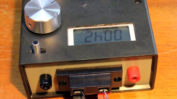
Current limited power supplies are a ubiquitous feature of the bench, and have no doubt helped prevent many calamities and much magic smoke being released from pieces of electronics. But for all their usefulness they are a crude tool that has a current resolution in the range of amps rather than single digit milliamps or microamps.
To address this issue, [Yann Guidon] has produced a precision current source, a device designed to reliably inject tiny currents. And in a refreshing twist, it has an extremely simple circuit in the form of a couple of PNP transistors. It has a range from 20 mA to 5 µA which is set and fine-tuned by a pair of pots, and it has a front-panel ammeter hacked from a surplus pocket multimeter, allowing the current to be monitored. Being powered by its own internal battery (and a separate battery for the ammeter) it is not tied to the same ground as the circuit into which its current is being fed.
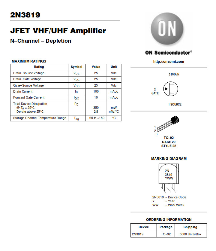
The 2N3819 is the archetypal general-purpose N-channel FET. (ON Semiconductor)
Over the recent weeks here at Hackaday, we’ve been taking a look at the humble transistor. In a series whose impetus came from a friend musing upon his students arriving with highly developed knowledge of microcontrollers but little of basic electronic circuitry, we’ve examined the bipolar transistor in all its configurations. It would however be improper to round off the series without also admitting that bipolar transistors are only part of the story. There is another family of transistors which have analogous circuit configurations to their bipolar cousins but work in a completely different way: the Field Effect Transistors, or FETs.
In a way it’s less pertinent to look at FETs in the way we did bipolar transistors, because while they are very interesting devices that power much of what you will do with electronics, you will encounter them as discrete components surprisingly rarely. Every CMOS device you deal with relies on FETs for its operation and every high-quality op-amp you throw a signal at will do so through a FET input, but these FETs are buried inside the chip and you’d be hard-pressed to know they were there if we hadn’t told you. You’d use a FET if you needed a high-impedance audio preamp or a low-noise RF amplifier, and FETs are a good choice for high-current switching applications, but sadly you will probably never have a pile of general-purpose FETs in the way you will their bipolar equivalents.
That said, the FET is a fascinating device. Join us as we take an in-depth look at their operation, and how and where you might use one.
FET basics
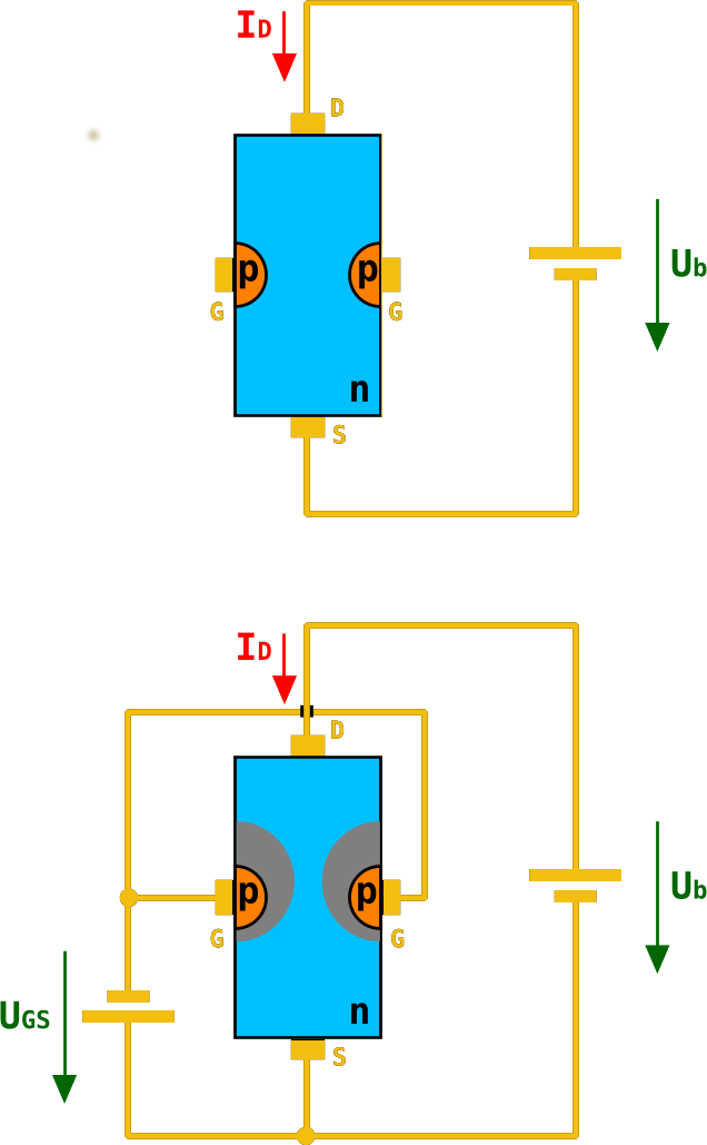
A diagram of an n-channel JFET. As the negative gate voltage on the p-type silicon decreases in the lower diagram, its electric field restricts the area through which electrons can flow in the n-type channel. Chtaube,(CC BY-SA 2.0 DE)
A basic FET has three terminals, a source (the source of electrons), a gate (the control terminal), and a drain (where electrons leave the device). These are analogous to the terminals on a bipolar transistor, in that the source fulfills a similar role to the emitter, the gate to the base, and the drain to the collector. Thus the three basic bipolar transistor circuit configurations have equivalents with a FET; common-emitter becomes common-source, common-base becomes common-gate, and an emitter follower becomes a source follower. It is dangerous to stretch the analogy between bipolar transistors and FETs too far, though, because of their different mode of operation. A closer similarity exists between a FET and a triode tube, if that helps.
The simplest FET for demonstration purposes has a piece of N-type semiconductor with source and drain connections at opposite ends, and a zone of P-type semiconductor deposited in its middle. This is referred to as an N-channel junction FET or JFET, because the channel through which current flows is N-type semiconductor, and because a diode junction exists between gate and channel. There are equivalent P-channel devices, just as there are PNP and NPN bipolar transistors.
Were you to bias an n-channel JFET as you would a bipolar transistor with a positive bias on its gate, the diode between gate and source would conduct, and the transistor would remain a diode with two cathode terminals. If however you give the gate a negative bias compared to the source, the diode becomes reverse-biased, and no current to speak of flows in the gate.
A characteristic of a reverse-biased diode is that it has a depletion zone between anode and cathode, an area in which there are no electrons. This is what causes the diode to no longer conduct, and the size of the depletion zone depends upon the size of the electric field that exists across it. If you’ve ever used a varicap diode, the capacitance between the two sides of this variable-width zone is the property you are exploiting.
In a FET, the depletion zone stretches from the gate region into the channel, and since its size can be adjusted by the gate voltage it can be used to “pinch” the remaining conductive region within the channel. Thus the area through which electrons can flow is controlled by the gate voltage, and thus the current that flows between drain and source is proportional to the gate voltage. We have an amplifier.
A simple FET radio receiver circuit showing FET biasing. The gate is biased at ground potential through the inductor, and the source is held above ground by the current in the 5K resistor. Herbertweidner [Public domain].In the JFET diagram above, the negative gate bias is represented by a battery. Tube enthusiasts may have encountered equipment that derives negative grid bias from a power supply, and you will find tube power units that include a -150 V rail for this purpose. In general though this is inconvenient in a FET circuit even though the voltage is lower, because of the extra cost of a negative regulator.. Instead the gate is held at a lower potential than the source by careful selection of a source resistor such that the current flowing through it brings the source up above ground, and a gate bias circuit that holds the gate close to ground. The base resistor chain from the bipolar circuit is for this reason often replaced with either a single resistor to ground, or a gate circuit with a very low DC resistance to ground such as an inductor.
MOSFETs, where the FET becomes more useful
Internal structure of an N-channel MOSFET. Fred the Oyster [Public domain].The JFET we have described is the simplest of field-effect devices, but it is not the one you will encounter most frequently. MOSFETs, short for Metal Oxide Semiconductor FETs, have a similar source, gate, and drain, but instead of relying on a depletion zone in a reverse-biased diode, they have a thin layer of insulation. The electric field from the gate acts across this insulation and pinches the conductive region in the channel through repulsion of electrons, with the same effect as it has in the JFET. It is beyond the scope of this piece to go into their mechanisms, but you will encounter two types of MOSFET: depletion mode devices that require the same negative bias as the JFET, and enhancement mode MOSFETS that require a positive bias.
Why would you use a FET?
So we’ve described the FET, and noted that while its mode of operation is different to that of a bipolar transistor it does a substantially similar job. Why would we use a FET then, what advantages does it offer us? The answer comes from the gate being insulated either by a depletion region in a JFET or by an insulating layer in a MOSFET. A FET is a voltage amplifier rather than a current amplifier, its input impedance is many orders higher than that of a bipolar transistor, and thus you will find FETs used in many applications that require a high impedance small-signal amplifier. The input of a high-performance op-amp will almost certainly be a FET, for example.
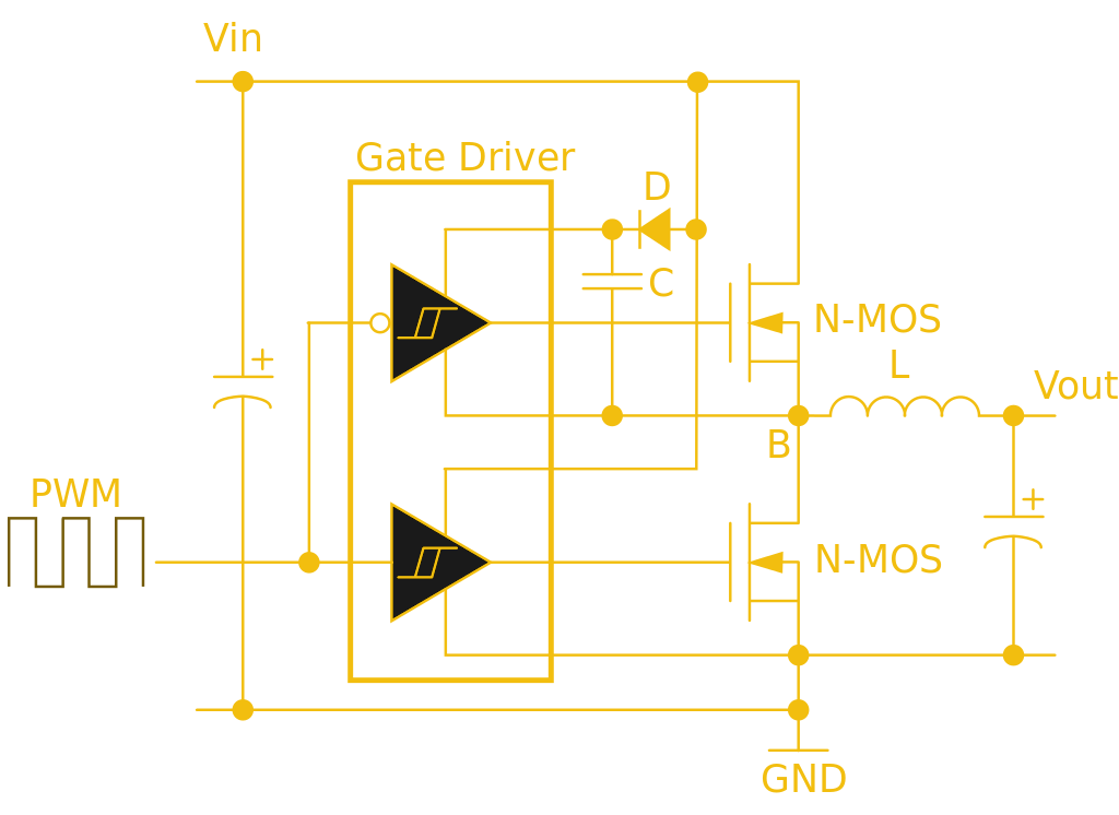
This half-bridge power MOSFET driver circuit uses a specialist gate driver IC with a pair of Schmidt buffers to deliver the initial surge required for a fast-turn-on time. Wdwd (CC BY 3.0).
The high input impedance has another effect less coupled to small signal work. Where a bipolar transistor requires significant base current to turn itself on, the corresponding FET requires almost none. Thus almost all complex integrated circuit logic devices are FET-based rather than bipolar because of the huge power saving that can be made by not needing to supply the base current demands of many thousands of bipolar transistors.
The same effect influences the choice of FETs for power switching, while a bipolar transistor’s base current is proportional to its collector current and thus it will need a significant driver, by contrast a power MOSFET requires virtually no standing gate current after an initial surge. A MOSFET power switch can thus be built requiring much less in the way of drive electronics and much more efficiently than a corresponding bipolar switch, and makes possible some of the tiny driver boards you might be used to for driving motors in your 3D printer, or your multirotor.
Through the course of this series you should have acquired a solid grounding in basic bipolar transistor principles, and now you should be able to add FETs to that knowledge base. We suggested you buy a bag of 2N3904s to experiment with in one of the previous articles, can we now suggest you do the same with a bag of 2N3819s?
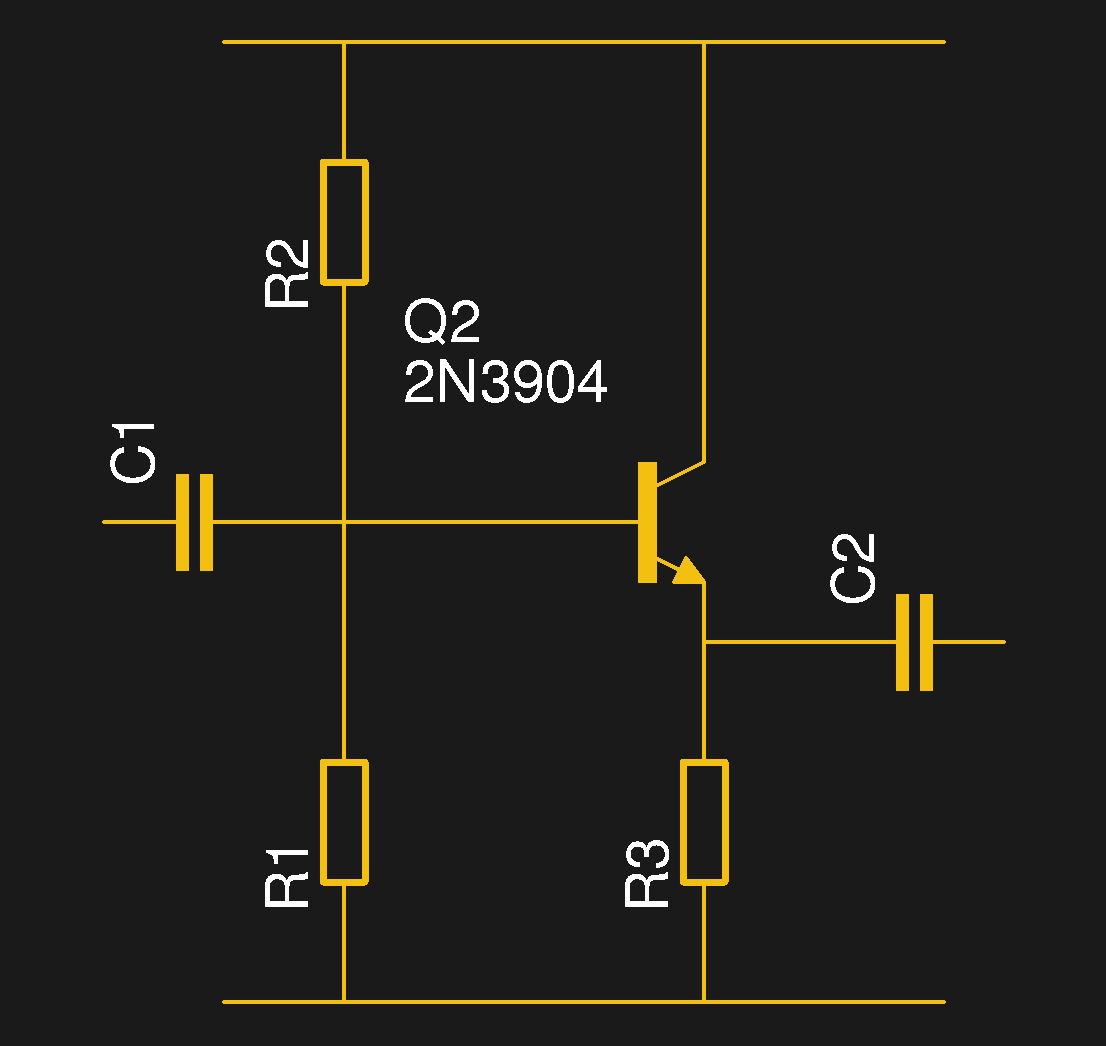
Just as the common emitter amplifier and common base amplifier each tied those respective transistor terminals to a fixed potential and used the other two terminals as amplifier input and output, so does the common collector circuit. The base forms the input and its bias circuit is identical to that of the common emitter amplifier, but the rest of the circuit differs in that the collector is tied to the positive rail, the emitter forms the output, and there is a load resistor to ground in the emitter circuit.
As with both of the other configurations, the bias is set such that the transistor is turned on and passing a constant current that keeps it in its region of an almost linear relationship between small base current changes and larger collector current changes. With variation of the incoming signal and thus the base current there is a corresponding change in the collector current dictated by the transistor’s gain, and thus an output voltage is generated across the emitter resistor. Unlike the common emitter amplifier this voltage increases or decreases in step with the input voltage, so the emitter follower is not an inverting amplifier.
Last time we looked at Spice models of a current sink. We didn’t look at some of the problems involved with a simple sink, and for many practical applications, they are perfectly adequate. However, you’ll often see more devices used to improve the characteristics of the current sink or source. In particular, a common design is a current mirror which copies a current from one device to another. Usually, the device that sets the current is in a configuration that makes it very stable while the other device handles the load current.
For example, some transistor parameters vary based on the output voltage which causes small nonlinearities in the output. But if the setting transistor has a fixed voltage across it, that won’t be a problem. The only problem with mirror schemes is that the transistors involved all have to match in key characteristics. For that reason, mirrors are usually better on ICs where the transistors are all more or less the same. You can get discrete transistors that have multiple devices built on a single substrate, but these are not very common.
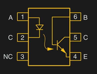
Deep in the heart of your latest project lies a little silicon brain. Much like the brain inside your own bone-plated noggin, your microcontroller needs protection from the outside world from time to time. When it comes to isolating your microcontroller’s sensitive little pins from high voltages, ground loops, or general noise, nothing beats an optocoupler. And while simple on-off control of a device through an optocoupler can be as simple as hooking up an LED, they are not perfect digital devices.
But first a step back. What is an optocoupler anyway? The prototype is an LED and a light-sensitive transistor stuck together in a lightproof case. But there are many choices for the receiver side: photodiodes, BJT phototransistors, MOSFETs, photo-triacs, photo-Darlingtons, and more.
So while implementation details vary, the crux is that your microcontroller turns on an LED, and it’s the light from that LED that activates the other side of the circuit. The only connection between the LED side and the transistor side is non-electrical — light across a small gap — and that provides the rock-solid, one-way isolation.


![A simple FET radio receiver circuit showing FET biasing. The gate is biased at ground potential through the inductor, and the source is held above ground by the current in the 5K resistor. Herbertweidner [Public domain].](https://hackaday.com/wp-content/uploads/2018/06/1kreiser_mit_fet.png)
![Internal structure of an N-channel MOSFET. Fred the Oyster [Public domain].](https://hackaday.com/wp-content/uploads/2018/04/n-channel_mosfet-svg1.png)

 But first a step back. What is an optocoupler anyway? The prototype is an LED and a light-sensitive transistor stuck together in a lightproof case. But there are many choices for the receiver side: photodiodes, BJT phototransistors, MOSFETs, photo-triacs, photo-Darlingtons, and more.


