A red hot crucible is held with metal tongs above a white plaster mold. The mold is held in a bright pink silicone sleve atop a metal pan on a wooden workbench. Red cheese wax holds the sleeve to a metal funnel connected to a vacuum cleaner.

Lost Print Vacuum Casting In A Microwave

Hacks are rough around the edges by their nature, so we love it when we get updates from makers about how they’ve improved their process. [Denny] from Shake the Future has just provided an update on his microwave casting process.

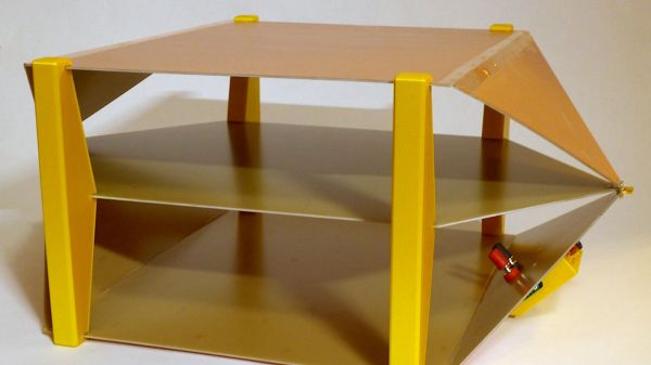
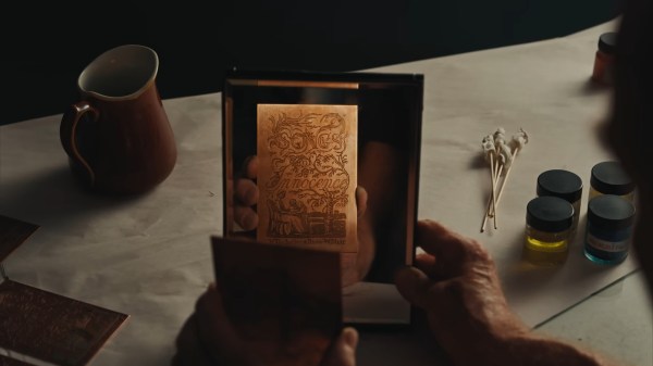
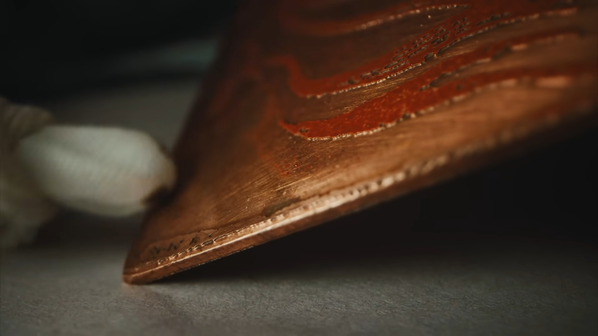
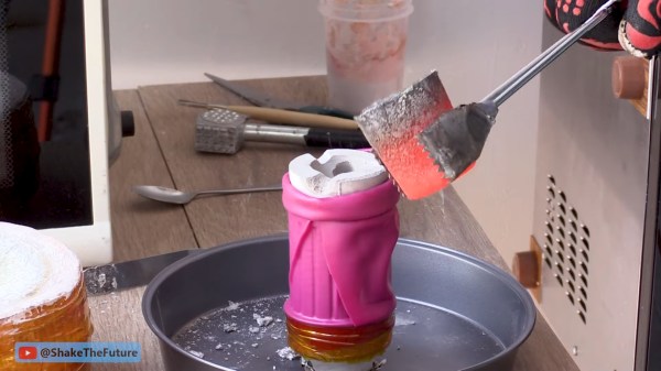
Sticking metal in a microwave certainly seems like it would be a bad idea at first, but with the right equipment it can work quite nicely to develop a compact foundry. [Denny] walks us through the process start to finish in this video, including how to build the kilns, what materials to use, and how he made several different investment castings using the process. The video might be worth watching just for all the 3D printed tools he’s built to aid in the process — it’s a great example of useful 3D prints to accompany your fleet of little plastic boats.A hand holds a very detailed copper ring. It is inscribed with the words "Open Source Hardware" and the open gear logo associated with open source hardware. It looks kinda like a class ring.

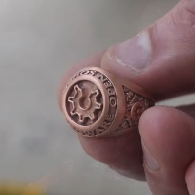
A lot of the magic happens with a one minute on and six minutes off cycle set by a simple plug timer. This allows a more gradual ramp to burn out the PLA or resin than running the microwave at full blast which can cause some issues with the kiln, although nothing catastrophic as demonstrated. Vacuum is applied to the mold with a silicone sleeve cut from a swimming cap while pouring the molten metal into the mold to draw the metal into the cavities and reduce imperfections.

We appreciate the shout out to respirators while casting or cutting the ceramic fiber mat. Given boric acid’s effects, [PDF] you might want to use safety equipment when handling it as well or just use water as that seems like a valid option.

If you want to see where he started check out this earlier version of the microwave kiln and how he used it to make an aluminum pencil.

Continue reading “Lost Print Vacuum Casting In A Microwave”

Homebrew TEM Cell Lets You EMC Test Your Own Devices

Submitting a new device for electromagnetic compatibility (EMC) testing seems a little like showing up for the final exam after skipping all the lectures. You might get lucky and pass, but it really would have been smarter to take a few of the quizzes to see how things were going during the semester. Similarly, it would be nice to know you’re not making any boneheaded mistakes early in the design process, which is what this DIY TEM cell is all about.

We really like [Petteri Aimonen]’s explanation of what a TEM cell, or transverse electromagnetic cell, is: he describes it as “an expanded coaxial cable that is wide enough to put your device inside of.” It basically a cage made of conductive material that encloses a space for the device under test, along with a stripline going down its center. The outer cage is attached to the outer braid of a coaxial cable, while the stripline is connected to the center conductor. Any electric or magnetic field generated by the device inside the cage goes down the coax into your test instrument, typically a spectrum analyzer.

[Petteri]’s homebrew TEM is made from a common enough material: copper-clad FR4. You could use double-sided material, or even sheet copper if you’re rich, but PCB stock is easy to work with and gets the job done. His design is detailed in a second post, which goes through the process of designing the size and shapes of all the parts as well as CNC milling the sheets of material. [Petteri] tried to make the joints by milling part-way through the substrate and bending the sheet into shape, but sadly, the copper didn’t want to cooperate with his PCB origami. Luckily, copper foil tape and a little solder heal all wounds. He also incorporated a line impedance stabilization network (LISN) into the build to provide a consistent 50-ohm characteristic impedance.

How does it work? Pretty well, it seems; when connected to a TinySA spectrum analyzer, [Petteri] was able to find high-frequency conductive noise coming from the flyback section of a switch-mode power supply. All it took was a ferrite bead and cap to fix it early in the prototyping phase of the project. Sounds like a win to us.

William Blake Was Etching Copper In 1790

You may know William Blake as a poet, or even as #38 in the BBC’s 2002 poll of the 100 Greatest Britons. But did you know that Blake was also an artist and print maker who made illuminated (flourished) books?

Blake sought to marry his art with his poetry and unleash it on the world. To do so, he created an innovative printing process, which is recreated by [Michael Phillips] in the video after the break. Much like etching a PCB, Blake started with a copper sheet, writing and drawing his works backwards with stopping varnish, an acid-resistant varnish that sticks around after a nitric acid bath. The result was a raised design that could then be used for printing.

Cleaning up the ink smudges before printing.

Blake was a master of color, using few pigments plus linseed or nut oil to create pastes of many different hues. Rather than use a brayer, Blake dabbed ink gently around the plate, careful not to splash ink or get any in the etched-away areas. As this was bound to happen anyway, Blake would then spend more time wiping out the etched areas than he did applying the ink.

Another of Blake’s innovations was the printing process itself. Whereas traditionally, illuminated texts must be printed in two different workshops, one for the text and the other for the illustrations, Blake’s method of etching both in the same plate of copper made it possible to print using his giant handmade press.

Want to avoid censorship and print your own ‘zines? Why not build a proofing press?.

Continue reading “William Blake Was Etching Copper In 1790”

This Packable Ham Radio Antenna Is Made From Nothing But Tape

On today’s episode of “Will It Antenna?”, [Ben Eadie (VE6SFX)] designs and tests an antenna made entirely of tape, and spoiler alert — it works pretty well.

By way of background, the basic design [Ben] uses here is known as a J-pole, a popular “my first antenna” design for amateur radio operators looking to go beyond the stock whip antenna that comes with that cheap handy-talkie you just can’t resist buying as soon as you get your license. Usually, though, hams will build their J-poles from rigid materials, copper water pipe being a typical choice. Copper has the advantage of being easily sourced, and also results in a self-supporting, weather-resistant antenna that’s easy to mount outdoors. However, copper is getting to be egregiously expensive, and a couple of meters of water pipe isn’t exactly amenable to portable operation, if that’s your jam.

To solve those problems, [Ben] decided to keep his copper use to a minimum with a roll of copper foil tape. He doesn’t provide any specs on the tape, but it looks like it’s about 6 mm (1/4″) wide and judging by a quick Amazon search, probably goes for about $10 a roll. He starts the build with a couple of strips of plain old duck tape — we’ve already had the “duck vs. duct” argument — laid out with the sticky sides together. The copper foil is applied to the duck tape backing using dimensions from any of the J-pole calculators available online. Dimensions are critical to getting good performance from a J-pole, and this is where [Ben]’s tape design shines. Element too long? No problem, just peel up a bit and tear some off. Did you go too far and make an element too short? Easy — just stick on an extension piece of foil. Tuning the location of the feedline connection was a snap, too, with movable terminals held in place with magnets.

Once everything was tuned up, [Ben] soldered down the feed points and covered the foil with a protective layer of duck tape. The antenna performed swimmingly, and aside from costing almost nothing to build, it weighs very little, rolls up to fit in a pack for field operations, and can easily be hoisted into a tree for better coverage. Looks like we’ll be putting in an order for some copper tape and building one of these too. Continue reading “This Packable Ham Radio Antenna Is Made From Nothing But Tape”

Copper Be Gone: The Chemistry Behind PCB Etching

For a lot of reasons, home etching of PCBs is somewhat of a dying art. The main reason is the rise of quick-turn PCB fabrication services, of course; when you can send your Gerbers off and receive back a box with a dozen or so professionally made PCBs for a couple of bucks, why would you want to mess with etching your own?

Convenience and cost aside, there are a ton of valid reasons to spin up your own boards, ranging from not having to wait for shipping to just wanting to control the process yourself. Whichever camp you’re in, though, it pays to know what’s going on when your plain copper-clad board, adorned with your precious artwork, slips into the etching tank and becomes a printed circuit board. What exactly is going on in there to remove the copper? And how does the etching method affect the final product? Let’s take a look at a few of the more popular etching methods to understand the chemistry behind your boards.

Continue reading “Copper Be Gone: The Chemistry Behind PCB Etching”

DIY Laser For Ablating Metal

For those who wish to go beyond through-hole construction on perfboard for their circuit boards, a printed circuit board is usually the next step up. Allowing for things like surface-mount components, multi-layer boards, and a wider array of parts, they are much more versatile but do have a slight downside in that they are a little bit harder to make. There are lots of methods for producing them at home or makerspace, though, and although we’ve seen plenty of methods for their production like toner transfer, photoresist, and CNC milling, it’s also possible to make them using laser ablation, although you do need a special laser to get this job done.

The problem with cutting copper is that it reflects infra-red, so a higher-wavelength blue green laser is used instead. And because you want to ablate the copper, but not melt the surrounding areas or cut straight through the board, extremely short, high-power pulses are the way to go. Here, the [Munich Fab Lab] is using 9 kW pulses of around 30 microseconds each.  With these specifications the copper is ablated from the surface of the board allowing for fine details in the range of about 20 µm, which is fine enough for just about any circuit board. The design of the laser head itself is worth a look.

Aside from the laser, the rest is standard CNC machine fodder, but with an emphasis on safety that’s appropriate for a tool in a shared workspace, and the whole project is published under an open license and offers an affordable solution for larger-scale PCB production with extremely fine resolution and without the need for any amounts of chemicals for the more common PCB production methods. There is a lot more information available on the project’s webpage and its GitHub page as well.

Of course, there are other methods of producing PCBs by laser if you happen to have a 20 W fiber laser just kicking around.

The Voltaic Pile: Building The First Battery

In the technologically-underpinned modern world, most of us interact with a battery of some sort every day. Whether that’s the starter battery in a car, the lithium battery in a phone, or even just the coin cell battery in a wrist watch, batteries underpin a lot of what makes society possible now. Not so in the early 1800s when chemists and physicists were first building and experimenting with batteries. And those batteries were enormous, non-rechargable, and fairly fragile to boot. Not something suited for powering much of anything, but if you want to explore what it would have been like to use one of these devices, follow along with [Christopher]’s build of a voltaic pile. Continue reading “The Voltaic Pile: Building The First Battery”